")
Silicon Nanowire FET
In this section we demonstrate some of M*’s capabilities by simulating the properties of a gate-all-around (GAA) silicon nanowire field-effect transistor (FET).
Nanowire (NW) FETs have been under study over the past decade due to their great potential as digital switches and are presently considered to be the most likely successor to planar and fin technologies. In this tutorial we simulate the electrical properties of a device design with an ultra-narrow channel comprised of a silicon nanowire of 3 nm in diameter, and a gate length of 10 nm. With present technology nodes already exhibiting features on the order of 10 nm – 50 nm, devices similar to the NW FET presented here may be a reality within the next decade.
M* performs device simulations based on fully quantum-mechanical electronic structure models in tandem with a non-equilibrium Green’s function (NEGF) approach for charge transport. M*’s implementation enables FAST simulation of device properties for quick turnaround design times; results presented in this section have been obtained in under 10 minutes using a single processor core on a modern laptop.
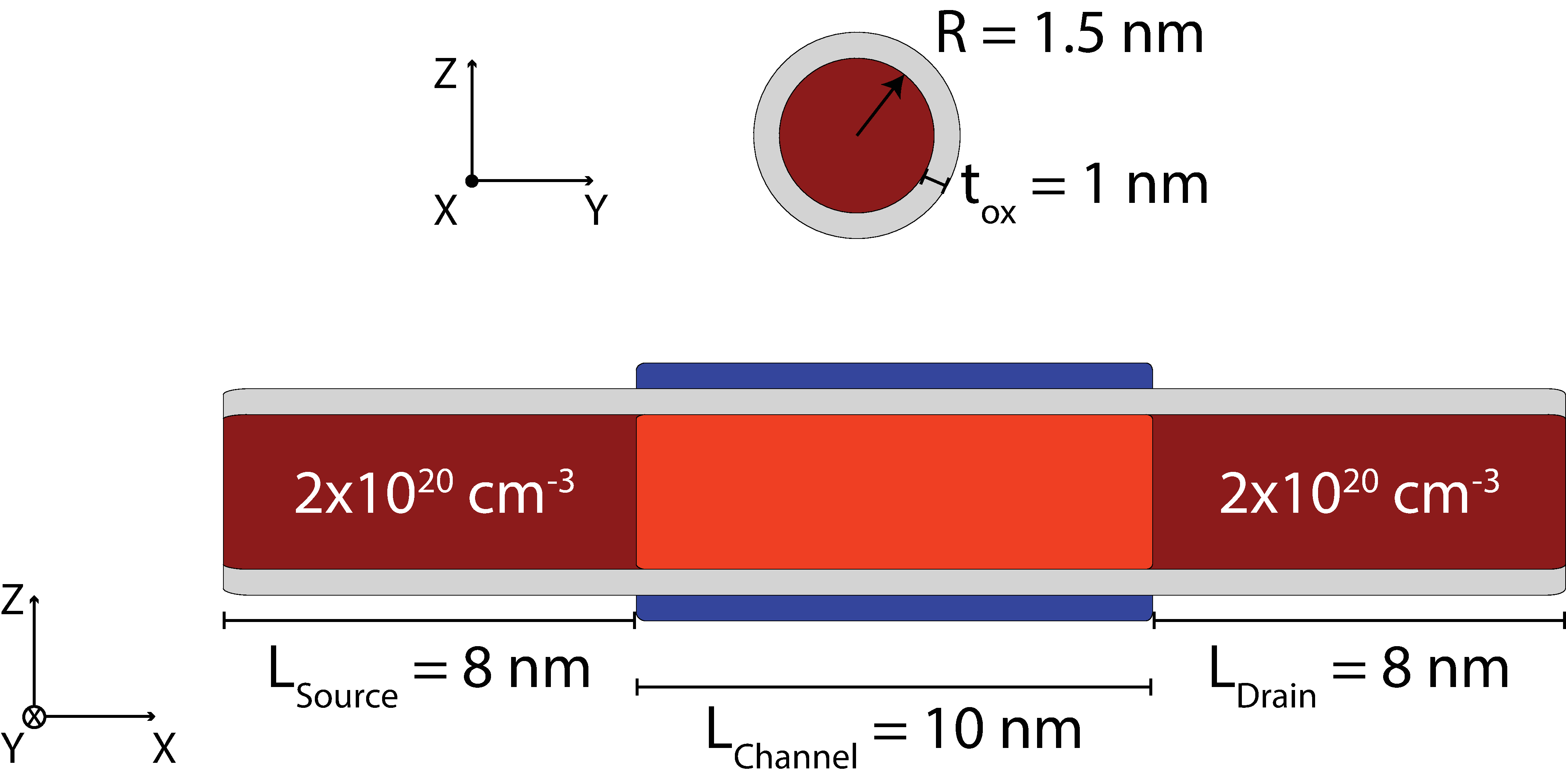
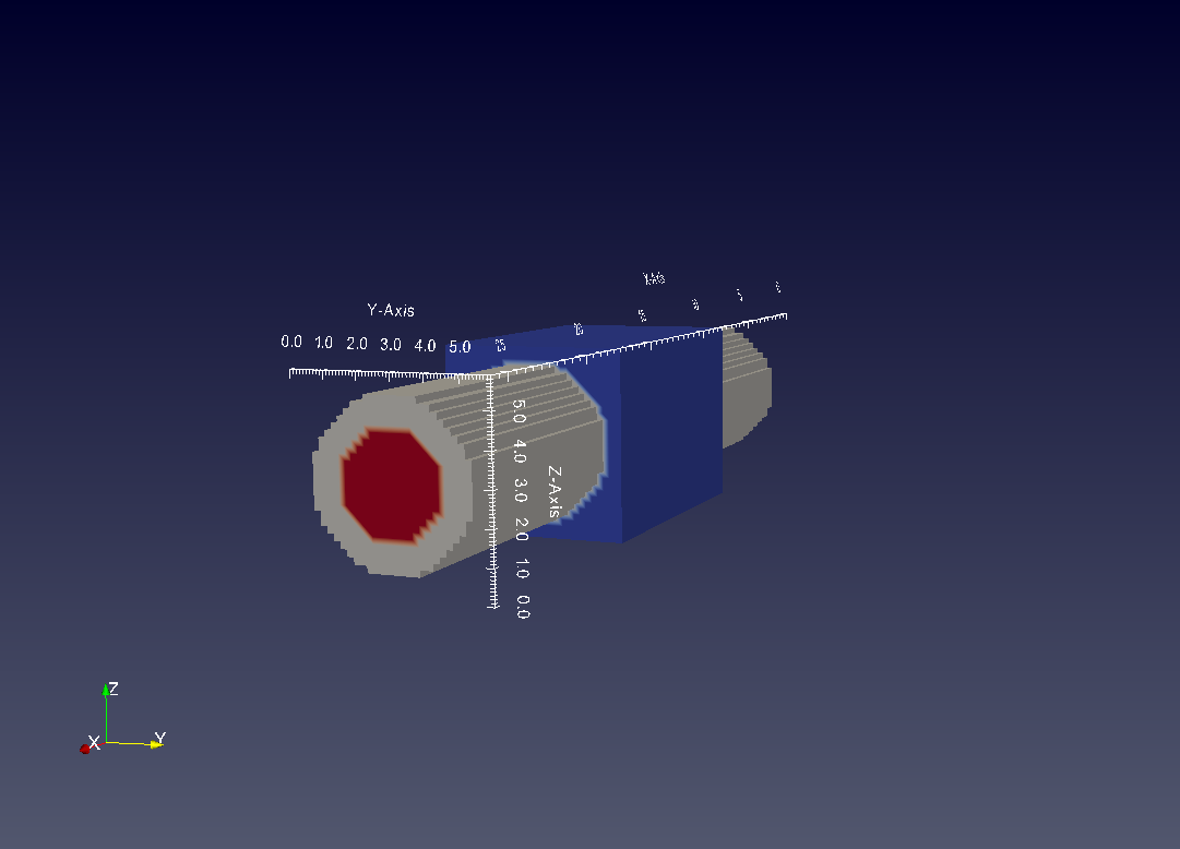
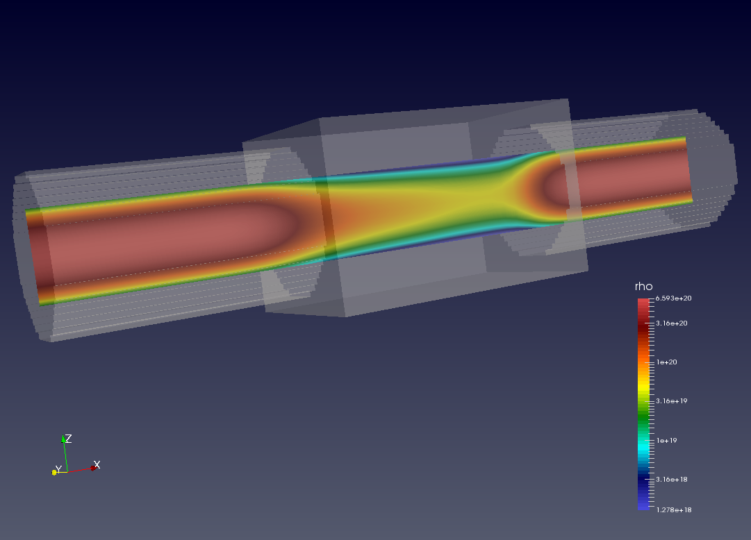
A schematic describing the geometry and doping profile of the device at hand is shown in figure 1. The device is comprised of a cylindrical [110] silicon NW with a radius of 1.5 nm surrounded by a 1 nm thick layer of silicon dioxide acting as gate oxide; a channel region is defined by a gate electrode surrounding the NW in a gate-all-around architecture. The wide contacts acting as the device’s source and drain are not explicitly modelled as they are assumed to be far away from the device channel and have perfect contact (i.e. ohmic contact) to narrow lead extensions located on either side of the channel, as per the usual NEGF framework.
In order to account for electrostatic screening and its effects on the device’s electrical properties, we explicitly model portions of the lead extensions closer to the gate electrode. The required length of lead extensions to be explicitly modeled depends on the materials comprising the device, its geometry and doping profile; for this design all properties are converged for lengths of 8 nm. Regions colored with varying shades of red in figure 1 highlight variations in the doping profile: the leads extensions are doped n-type to a free electron concentration of 2×10²⁰ N / cm3 while the region under the gate is considered to be intrinsic with a much lower carrier concentration, which we shall neglect.
Input files required for a corresponding M* simulation can be prepared with the M* Graphical User Interface (GUI). Figure 2 shows different sections of M*’s GUI along with input values describing the SiNW device.
- The Geometry and grid properties tab defines the device as a cylindrical NW in a GAA architecture with three distinct regions, and sets appropriate grid spacings
- The Material properties tab describes the properties of the conduction-band valleys and permittivity of each region
- The Control tab allows defining the type of voltage sweep and its limits, type of scattering to be considered in the simulation, convergence parameters, and files to be output
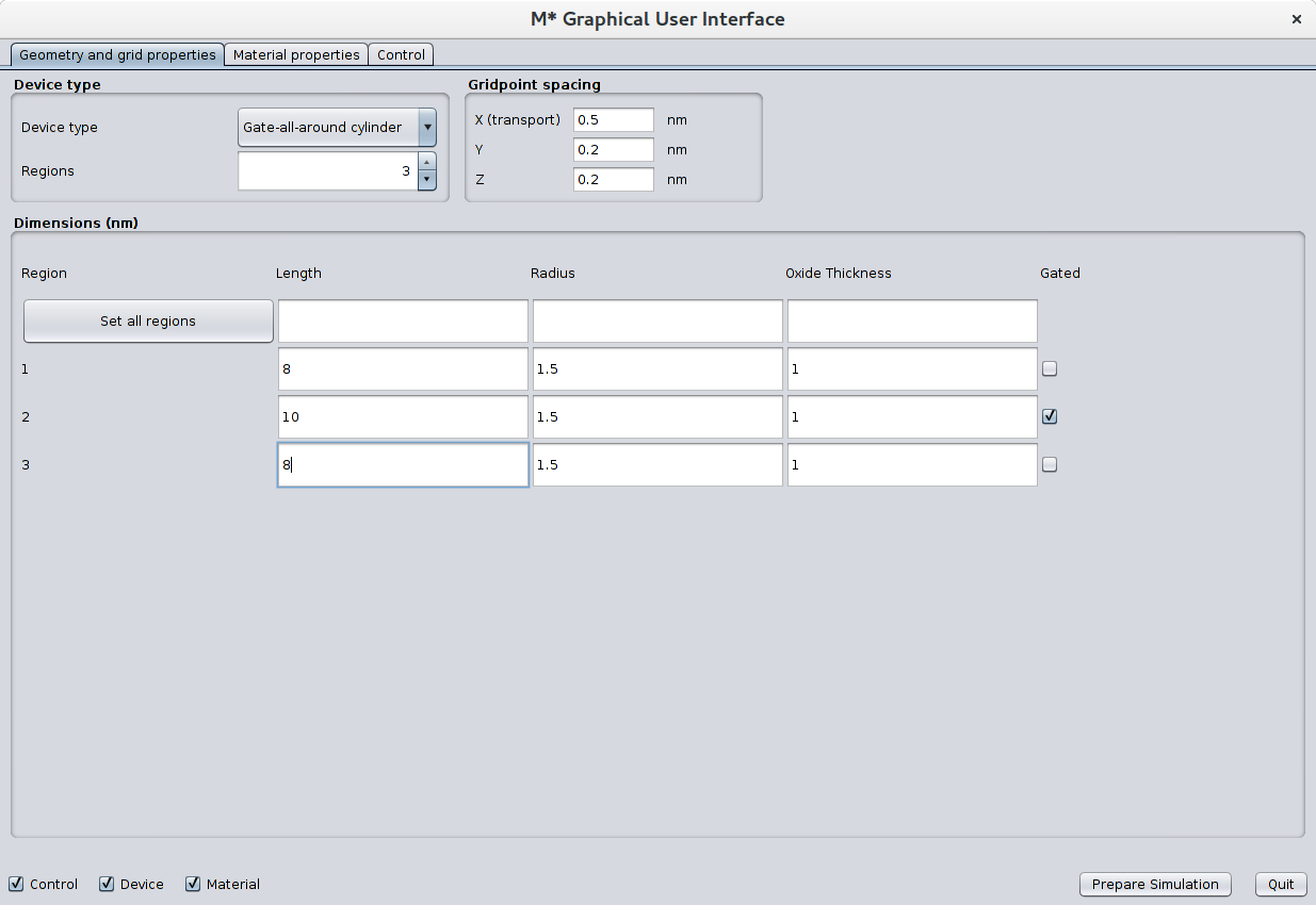

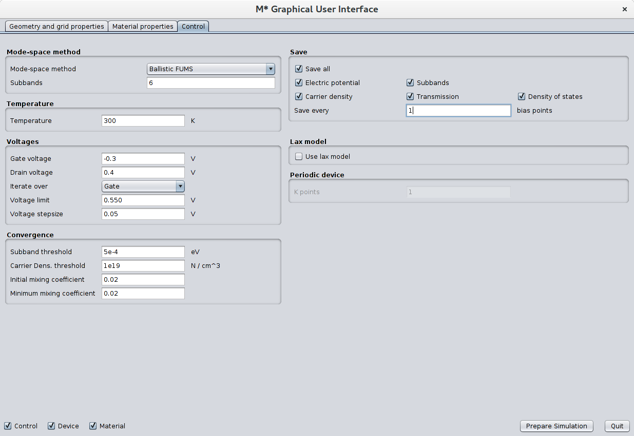
Figure 2: M* GUI setup employed for SiNW FET simulations.
We neglect all sources of electron scattering and simulate the device in the ballistic regime, a reasonable approximation given its short length. This type of simulation quickly provides information on the device’s properties as defined by its geometry and intrinsic material properties, thus allowing exploration of performance limits when sources of scattering detrimental to device operation such as electron-phonon interactions are not accounted for.
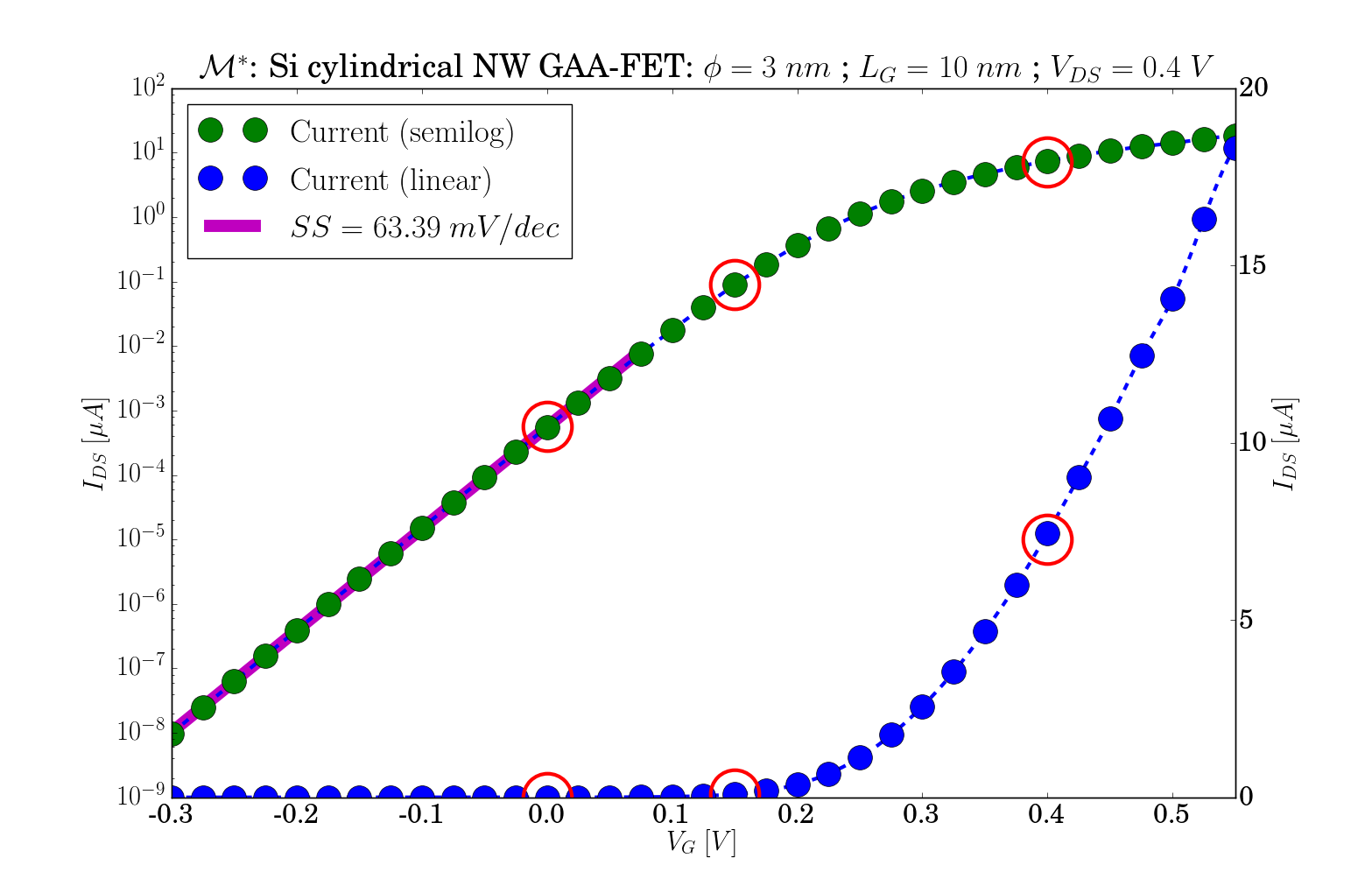
Figure 3 shows the device’s transfer characteristics on semilog and linear scales for a drain-source bias of VDS = 0.4 Volts. A least-squares fit results in a predicted subthreshold swing (SS) of 63.39 mV/dec, indicating excellent switching characteristics with a SS value near the thermodynamic lower limit.
In figure 3 we have highlighted in red circles three bias points corresponding to OFF, ON, and SAT (saturation) states which we take as representative of each device operation regime for exploring evolution of other quantities shown below.
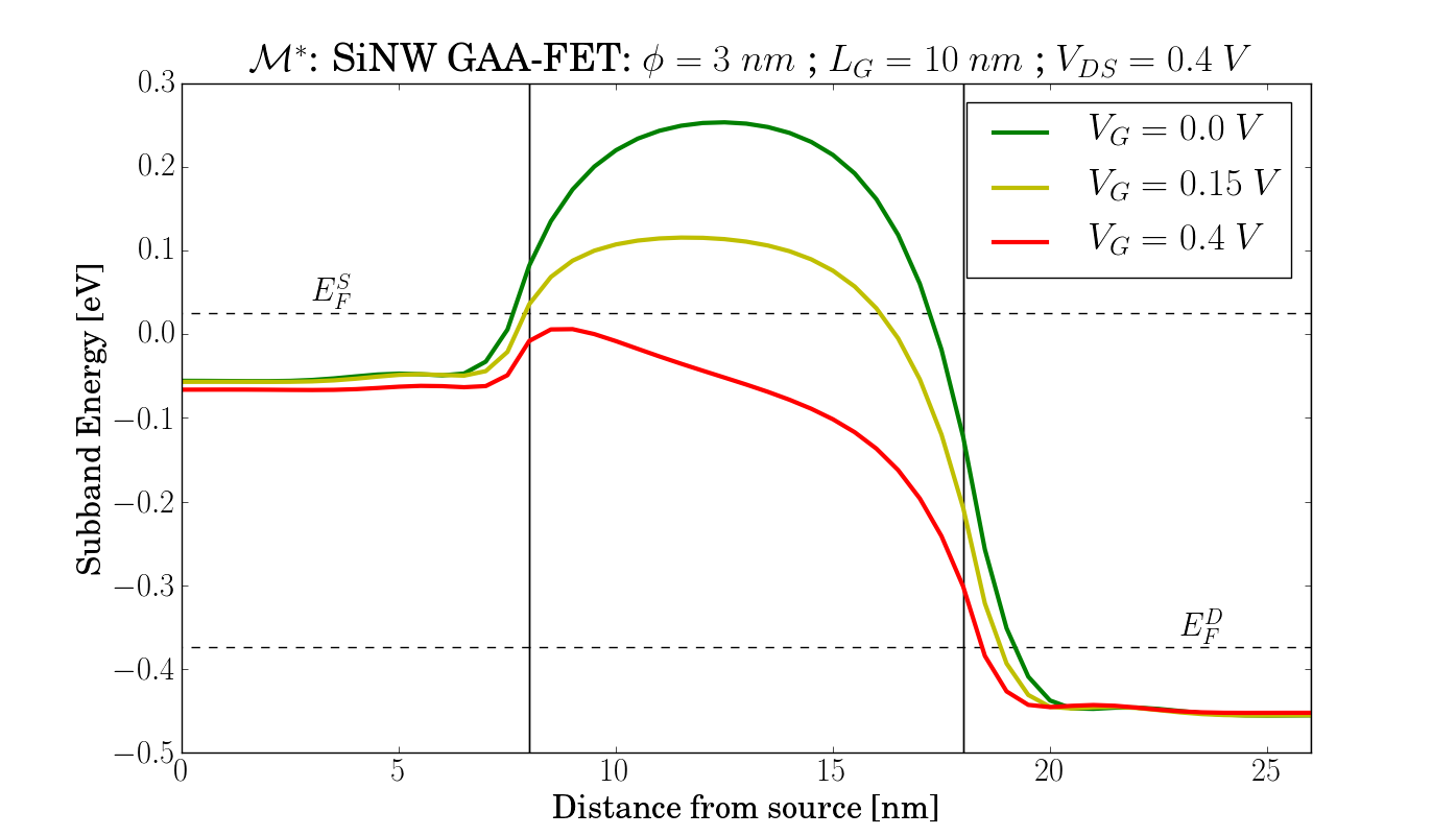
Figure 4 shows the lowest subband in energy across the device when in its OFF state (green), ON state (yellow), and in saturation regime (red).
It can be seen how the barrier encountered for electrons coming from the source (left hand side in the figure) is reduced for increasing values of gate bias, thus allowing larger currents to flow through the channel. While the barrier induced in the channel region in its OFF state is around 250 meV above the source Fermi level ( ~10 × κBT at room temperature ) and severely impedes current flow, the first subband lies below the source Fermi level across the whole device when in saturation regime so electrons can easily flow through it.
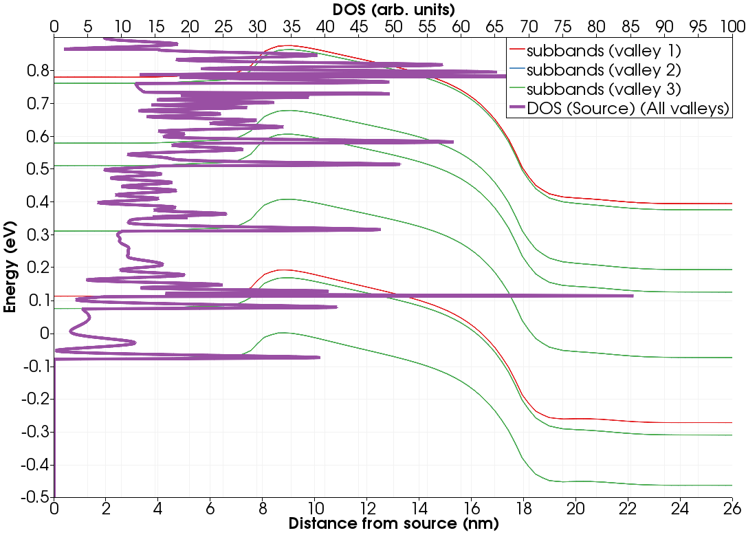
M* enables comprehensive analysis of simulated devices’ electronic structure by allowing extraction, visualisation, and overlaying a number of results such as of density of states, subband profiles, and transmission probabilities associated to each conduction valley and device region, as depicted in figure 5.
![]()
Figure 5: Subband profile, density of states at the source region, and transmission probability function for carriers in a particular conduction valley.
Additionally, you may plot the carrier density and electrostatic potential across the device as 3D grids for a better understanding of how they correlate and ultimately gain insight into device operation and design optimisation based on simulations based on quantum mechanical models.
To learn more about M*’s features and capabilities or to request a demo version, don’t hesitate to contact us