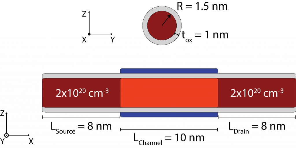
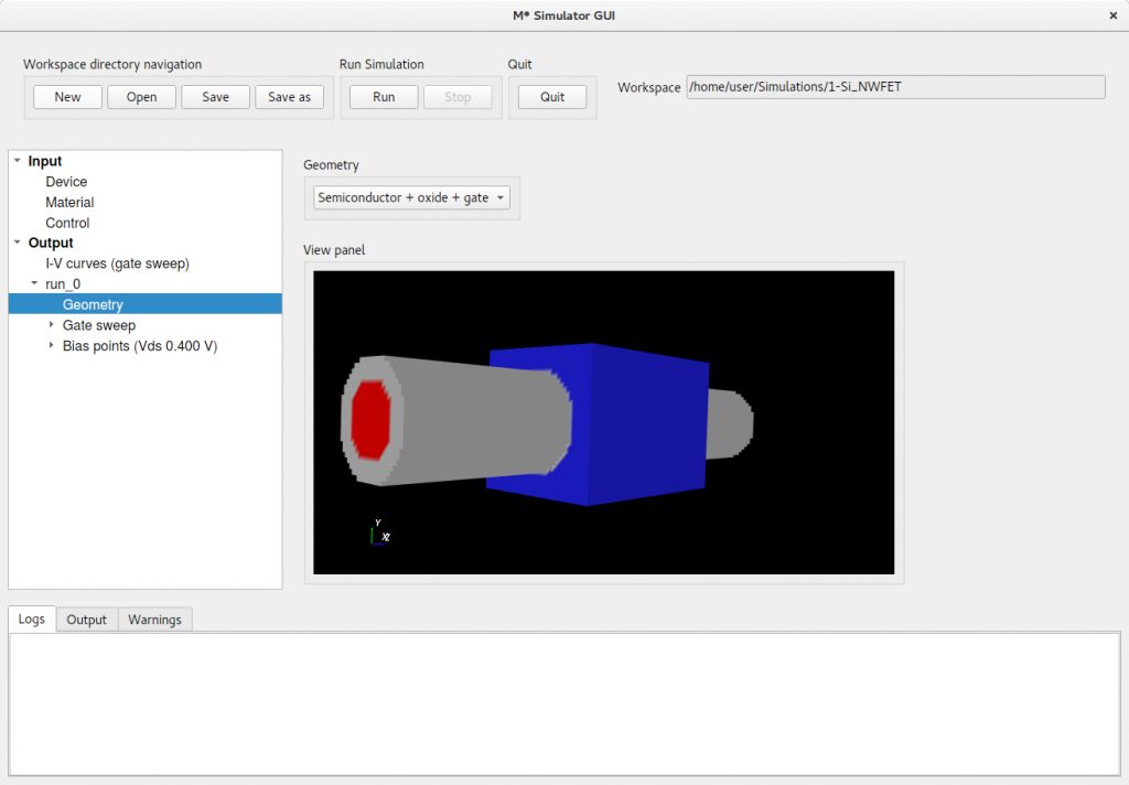
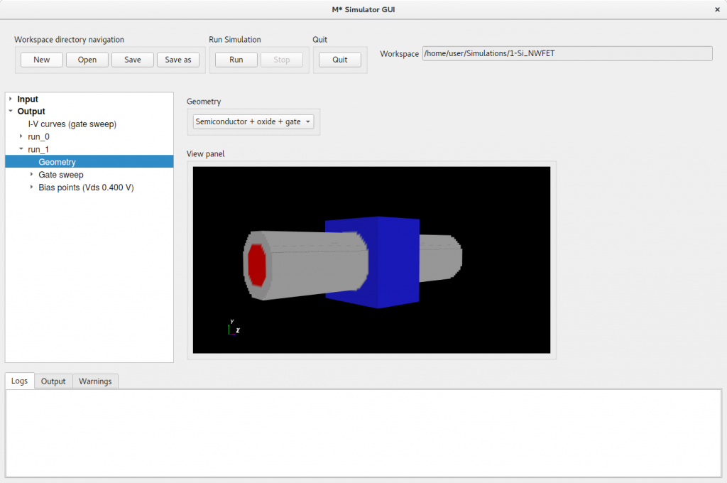
Figure 1:Schematic showing device geometry. Red represents silicon, gray represents silicon dioxide, and blue the gate electrode. Regions in different shades of red represent variations in doping across different device regions.
This section illustrates the process of preparing, running, and analysing a simulation of a silicon nanowire field-effect transistor (Si NWFET) with homogeneous geometry along its transport axis (i.e. constant cross-section) by employing the ballistic FUMS method. We shall simulate a silicon 〈100〉 gate-all-around device with cylindrical cross-section and a radius of 1.5 nm, a channel length of 10 nm, and 8 nm long source/drain extension regions. Figure 1 shows a schematic of the device geometry, highlighting variations in the doping profile across the silicon portion of the nanowire with different shades of red. Source and drain regions are doped n-type with a carrier concentration of 2 × 10²⁰ N/cm3 while the channel is intrinsic with a much lower carrier density, which we shall neglect and take to be zero.
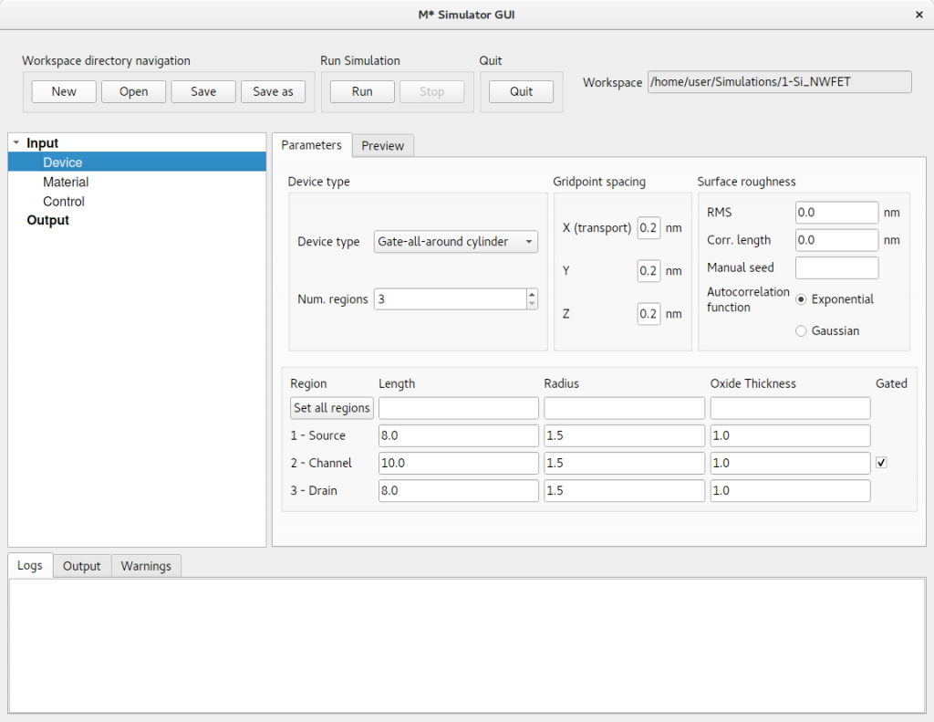
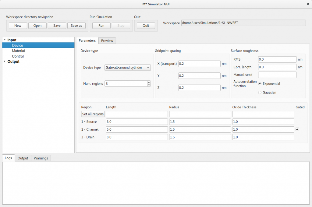
In order to begin preparing the input files for simulating this device, launch the M* GUI, click New and choose a folder to save your results to. Navigate to the Device panel on the left pane and set device geometry parameters as described in figure 1 by filling out values as shown in figure 2. Leave Gridpoint spacing and Surface roughness fields to their default values. You may switch to the Preview tab to visualise the device structure and ensure it corresponds to your intended design.
Figure 2:In the Device panel, specify a Gate-all-around cylinder with 3 regions, with dimensions shown above. Make sure region 2 (i.e. the device channel) is Gated.
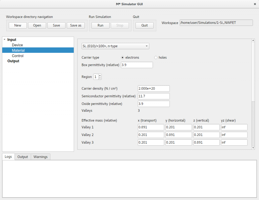
Once you have completed filling out the Device panel, select Material in the left pane to enter the material properties for each region. Select Si, (010)〈100〉, n-type from the dropdown menu to select the device’s semiconductor material across all regions. (Note:Although M* supports simulating devices with different materials in different regions, it requires manual editing of input files as the current version’s GUI does not include support for building devices with heterogeneous materials. Selecting a material anywhere in the Material panel sets the main electronic structure properties for all regions.) Cycle through regions 1 – 3 using the region spinner and ensure the oxide permittivity is set to 3.9 –the relative permittivity of silicon dioxide–, and Carrier density values are set as 2×1020 cm-3 and for source and drain regions (regions 1 and 3) and 0.0 for the channel region (region 2). Figure 3 shows values set for the source region.
Figure 3:In the Material panel, cycle through regions 1 – 3 and ensure oxide permittivity is set to 3.9, and Carrier density values are set as 2×1020 cm-3 for source and drain regions (regions 1 and 3), and 0.0 for the channel region (region 2).
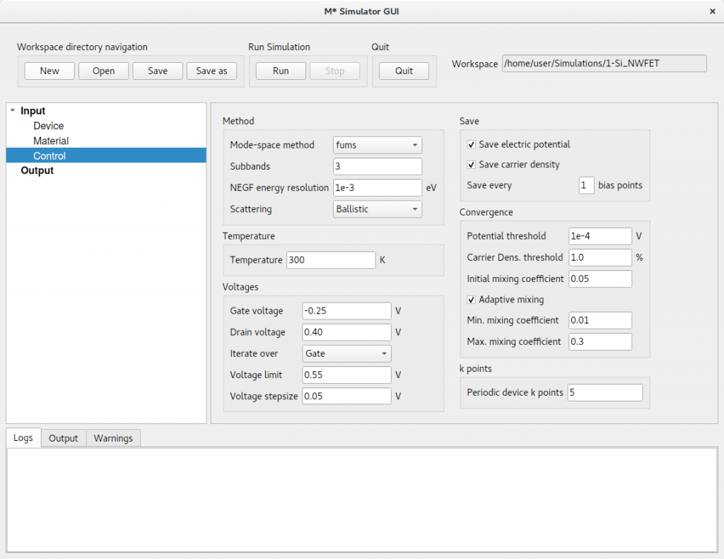
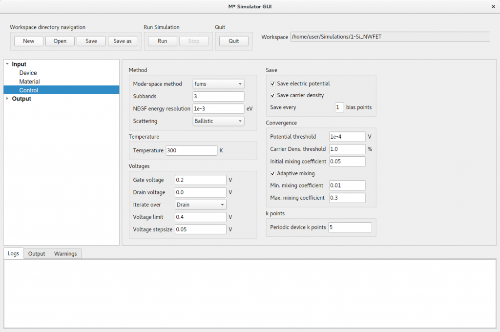
To finish setting all input parameters for our simulation, select Control on the left pane and fill out values as shown in figure 4:
Method select the fast uncoupled mode-space method –suitable for devices with both homogeneous and small cross-sections–, with 3 subbands per valley and Ballistic scattering
Temperature leave a value of 300 K (26.85 °C)
Voltages input a Drain voltage of 0.40 V and a Gate voltage of -0.25 V. Select Iterate over -> Gate, input a Voltage limit of 0.550 V and a Voltage stepsize of 0.05 V to indicate a gate bias sweep in the [-0.25,0.55] V range, in steps of 0.05 V
Save enable saving of both electric potential and carrier density, and set Save every to 1 so data is saved for all bias points computed
Convergence set the Potential threshold to 10-4 eV, Carrier Dens. threshold to 1%, and the Initial mixing coefficient to 0.05. Enable Adaptive mixing and set the minimum and maximum coefficients to 0.01 and 0.3, respectively
Figure 4:In the Control panel, fill out fields with values shown in the figure.
Once you have finished setting all input variables, you are now ready to launch your first M* simulation: click Run at the top pane of the GUI to begin. Once your simulation has been started, a subfolder will be created inside your current workspace directory where all associated output files will be saved. You can follow simulation progress in the tabs located at the bottom pane of the GUI:
Logs shows the contents of the M* logfile, which is also saved to your simulation folder under the filename mstar_log.out. It contains a header with information about the simulated device and subsequently includes useful information on simulation progress. After each iteration, M* will write a line with six columns to this file with the following quantities:
Iter: iteration index for the present bias point
Vds (V): drain-source bias in volt
Vgs (V): gate-source bias in volt
Ids (A): drain-source current in ampere
R[Q] (%): charge residue in percentage with respect to that iteration’s input charge density
dV (V): maximum difference in electric potential between the last two iterations in volt
Output shows M*‘s standard output stream stdout. After each iteration, the contents of this tab will get updated with the following information:
Method: mode-space method employed
Drain-source bias: drain-source bias in volt
Gate-source bias: gate-source bias in volt
Drain current: drain current in ampere
Potential convergence: maximum difference in electric potential between the last two iterations followed by the requested convergence threshold in parenthesis, both in volt
Density convergence: charge residue in percentage with respect to that iteration’s input charge density, followed by the requested convergence threshold in parenthesis
Linear mixing coeff: mixing coefficient used in the present iteration
Warnings shows M*‘s standard error stream stderr, containing any errors or warnings that occur during the simulation
When the simulation has finished, both Logs and Output tabs will show a summary of the time taken to run the simulation, with the time spent in each M* module indicated. You may then begin analysing results (Note: Results for each bias point become available for analysis as soon as they have been converged) by expanding the Output section on the left pane to show a list of runs performed so far in the current workspace. Every simulation launched by clicking the Run button will be listed under the default name run_〈N〉, with 〈N〉 an incremental index (e.g. run_0, run_1, etc.), and the corresponding output data will be saved to subfolders with the same name. Expand the item labelled run_0 to list output quantities associated with the simulation just performed:
Figure 5:Once your simulation has finished running, expand the Output section on the left pane to list all available runs; select run_0 to list all output corresponding to the first simulation just completed. Clicking Geometry displays a 3D render of the simulated device geometry.
Geometry allows visualising a 3D render of the simulated device geometry, as shown in figure 5. A drop-down menu allows choosing between visualising only the semiconductor region, the semiconductor and oxide regions, or all regions including semiconductor, oxide, and gate electrode. You may rotate the 3D model using your mouse’s left click button, zoom in or out by holding your mouse’s right click button, pan using your mouse’s middle button (or shift + left click), and spin using ctrl + left click
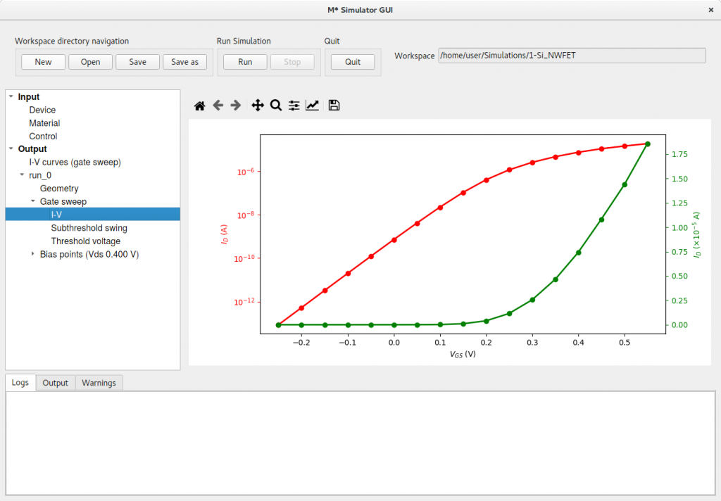
Figure 6:Device transfer characteristics are displayed as both semilogarithmic (red, left vertical axis) and linear plots (green, right vertical axis).
Gate sweep expand this item to list the following output available for gate sweep runs:
I-V displays a plot of the device’s transfer characteristics as both semilogarithmic and linear plots, as shown in figure 6. The toolbar at the top of all 2D plots in M* allows customising the look of the plot and save it as an image file in various formats
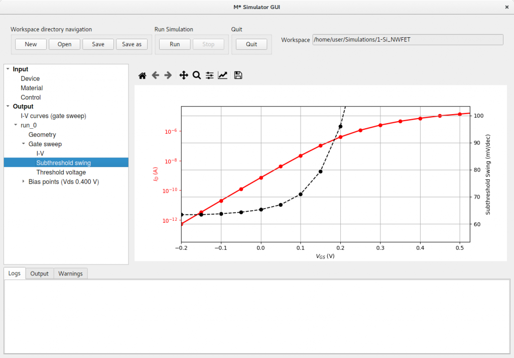
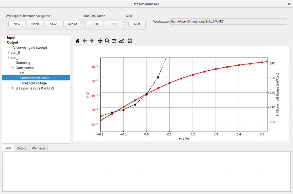
Figure 7:Subthreshold swing’s dependence with gate bias. This device exhibits values below 70 mV/dec for gate voltages below 0.1 V.
Subthreshold swing select this item to display a plot showing the ID – VGS characteristics (semilogarithmic, left vertical axis) and the subthreshold swing computed at each gate bias. As shown below in figure 7, this device exhibits excellent characteristics with a subthreshold swing below 70 mV/dec for gate voltages below 0.1 V
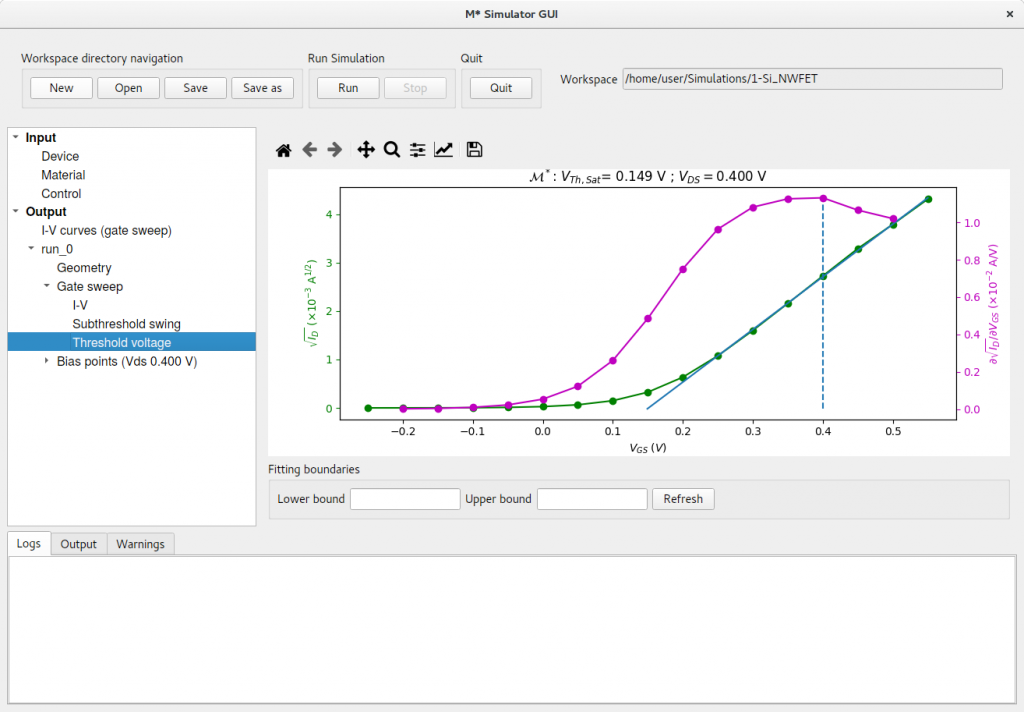
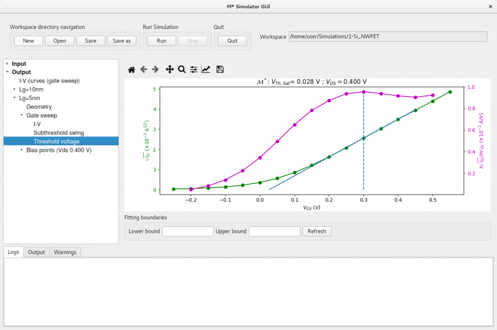
Figure 8:The device’s threshold voltage extracted using the linear extrapolation method.
Threshold voltage lists all gate bias sweep runs detected in your simulation folder, similar to the previous item in this list. Click on this item to display a plot illustrating the extraction of the device’s threshold voltage using the linear interpolation method. Two variations of the method will be employed depending on whether the device is considered to be operating in its linear region (VDS 〈 0.1 V) or in its saturation region (VDS ≥ 0.1 V). The computed threshold bias is the value of VGS at which the blue line intersects the origin of the vertical left axis (shown in green). The blue line is computed using the slope of the green curve at the point where the magenta curve reaches its maximum value; indicated with a dashed vertical line (see figure 8)
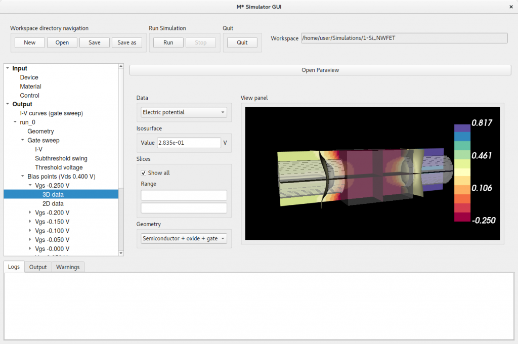
Figure 9:3D data panel displaying electric potential data with the device’s geometry overlaid.
Bias points (Vds 0.400 V) lists all bias points for which output data has been saved to disk. Expand this item to list gate voltages included in the present run –for which drain voltage has been kept to Vds 0.400 V–; expanding items associated with each gate voltage will reveal two sub-items:
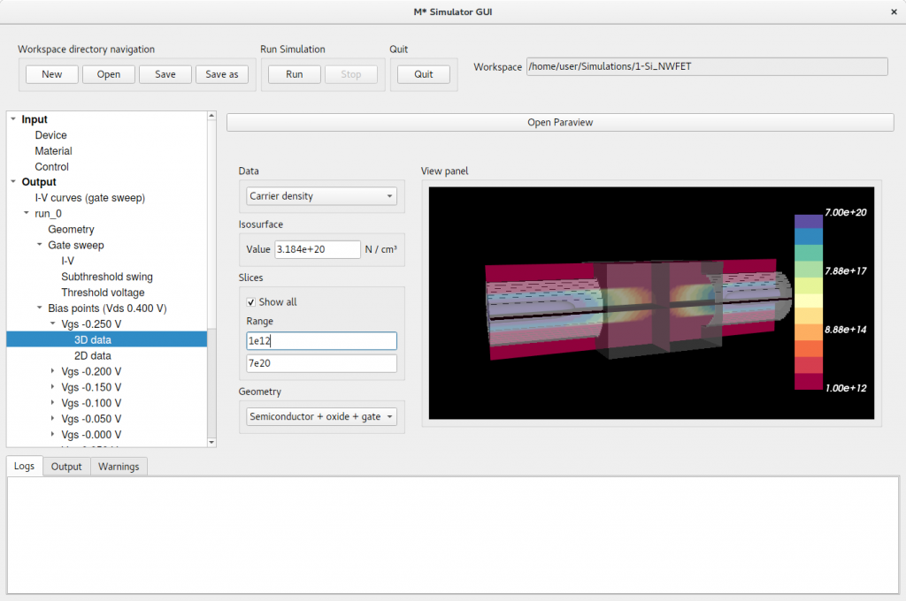
3D Data: allows visualising the electric potential or carrier density on 3D grids. Select this item to show a 3D render of the electric potential with a semitransparent device geometry overlaid (figure 9). The render will show an isosurface for the value input in the corresponding field while contour plots for slices along each cartesian axis are displayed upon ticking Slices - Show all; the limits of the colourmap can be manually set using the Range field. Displaying various elements of the device geometry can be controlled via the Geometry dropdown menu. You may select Carrier density in the Data dropdown menu to display a 3D render of that quantity instead, with similar controls available (figure 10). Clicking the Open Paraview button at the top of this panel will display the 3D data in ParaView, a software package which allows further manipulation and visualisation options should you require so.
Figure 10:3D data panel displaying carrier density data with the device’s geometry overlaid. Note the limits of the colourmap have been manually set using the Range fields.
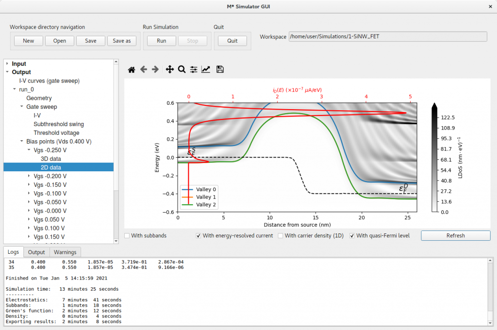
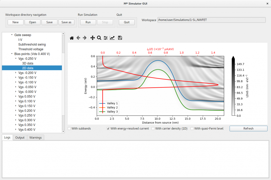
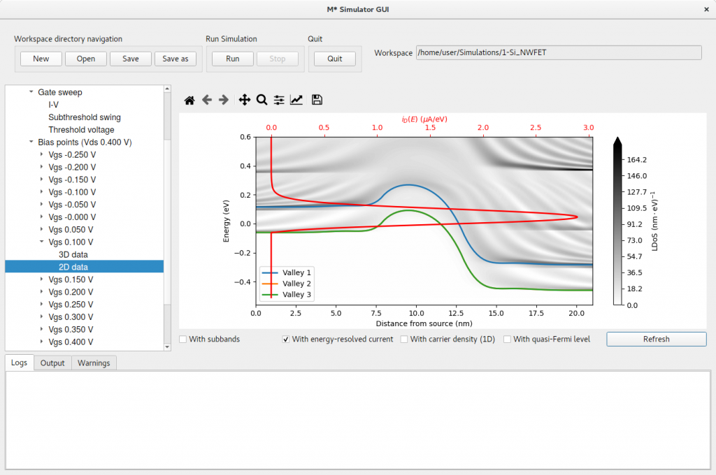
2D data: displays a contour plot of the local density of states (LDoS) and line plots indicating band edges for each valley. Additional quantities may be overlaid by ticking the corresponding tickboxes below the plot and clicking the Refresh button, as shown in figure 11
Figure 11:2D data panel displaying local density of states, energy-resolved current, and quasi-Fermi level data for an OFF state.
With these visualisation and post-processing tools you may study a device design’s figures of merit, and their dependence with various geometrical, electrical, and material parameters. Let us now explore the effects of reducing the gate length from 10 nm to 5 nm on the threshold voltage and subthreshold swing by running a gate sweep simulation with appropriate modifications to the device geometry: Select Input -> Device, change the length of region 2 as shown in figure figure 12 and click Run.
Figure 12:Reduce the length or region 2 from 10 nm to 5 nm in the Input -> Device panel and click Run to study the impact of reducing the device’s channel length.
After this second simulation has completed, you will find its results listed under Output->run_1 in the left pane, as shown in figure 13. Note you can find all input and output data associated with each run in your workspace’s subdirectories run_0 and run_1. Navigate to the Subthreshold swing and Threshold Voltage panels of run_1 to observe the impact of reducing the device’s gate length in both quantities: the subthreshold swing degrades to values above 100 mV/dec (figure 14), and the threshold voltage is reduced to approximately 30 mV in what is known as threshold voltage roll-off (figure 14).
Figure 13:Once the second simulation with the reduced gate length finishes, you will find its output listed as run_1.Figure 14:Reducing the device’s gate length results in an increase of the subthreshold swing.Figure 15:Reducing the device’s gate length results in a shift of the threshold voltage towards a lower gate bias. Note simulations listed on the left pane have been renamed to more descriptive names.
Renaming simulations
By default, your simulations are labelled using the sequence run_0, run_1, run_2, etc. You may relabel them to something more convenient by either double-clicking their label or selecting the label on the left pane and pressing F2 on your keyboard, and typing a new label. The corresponding subfolder within your workspace will be renamed accordingly.
To facilitate identifying runs performed so far let us rename run_0 to Lg=10nm and run_1 to Lg=5nm, as shown in figure 15.
Comparing gate sweeps
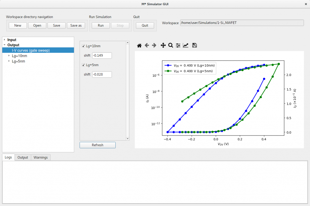
We may directly explore the effects of reducing the device’s gate length on its transfer characteristics using the Output->I-V curves (gate sweep) panel, as shown in figure 21. You may select which runs to include in the plot by activating the corresponding tick boxes on the list and clicking the Refresh button below.
Comparing data for both runs we can observe the aforementioned threshold voltage roll-off, as well as a significant increase in OFF currents when reducing the device’s channel length. The latter can be attributed to increased source-to-drain tunnelling observed in the shorter channel device’s OFF states, as evidenced by the energy-resolved current (red curve) in figure 17 where most electron transport is located at energies below the channel’s band edge. This can be contrasted against the longer channel device’s, where the largest contribution to OFF current occurs at energies above the channel’s band edge (figure 11).
Figure 16:The Output->I-V curves (gate sweep) panel allows shifting curves along the horizontal axis for more meaningful comparisons. The horizontal axis’ label has been manually set to VOV using the toolbar at the top of the plot.
In order to make this comparison more meaningful, let us shift their ID-VGS characteristics by their respective threshold voltages to represent the overdrive voltage along the horizontal axis: VOV = VGS – VTh. To do so, type each device’s -VTh,Sat (with opposite sign) into their corresponding shift fields to align their threshold voltage with the horizontal axis’ origin. Click Refresh to generate a plot similar to figure 16. The horizontal axis’ label has been manually set to VOV using the toolbar at the top of the plot.
An additional feature becomes apparent after shifting both curves: the device with shorter gate length exhibits decreased ON current when compared to the device with LG = 10 nm at the same overdrive voltage. This is a consequence of larger tunnelling contributions to ON current in the shorter device, as can be seen in figure 18.
Figure 17:The shorter channel length device’s 2D data reveals a stronger source-to-drain tunnelling contribution to OFF currents.Figure 18:The shorter channel length device’s 2D data reveals a strong source-to-drain tunnelling contribution to ON currents.
Drain sweeps
We continue by exploring the case of simulating a family of drain current curves by computing ID – VDS characteristics at three different gate voltages. Select Input -> Control on the left pane and modify the Voltage section as (see figure 19):
Gate voltage: start by simulating a curve with a gate voltage of 0.2 V
Drain voltage: set the starting drain voltage to 0.0 V
Iterate over: select Drain from the dropdown menu
Voltage limit: set the maximum drain voltage in your sweep to 0.4 V
Voltage stepsize: leave this value set to 0.05 V
Figure 19:Modify the Input->Control panel to set up a drain sweep simulation.
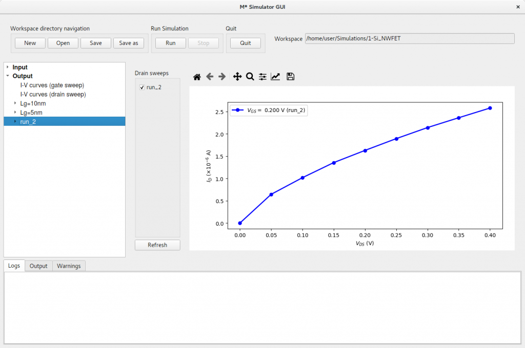
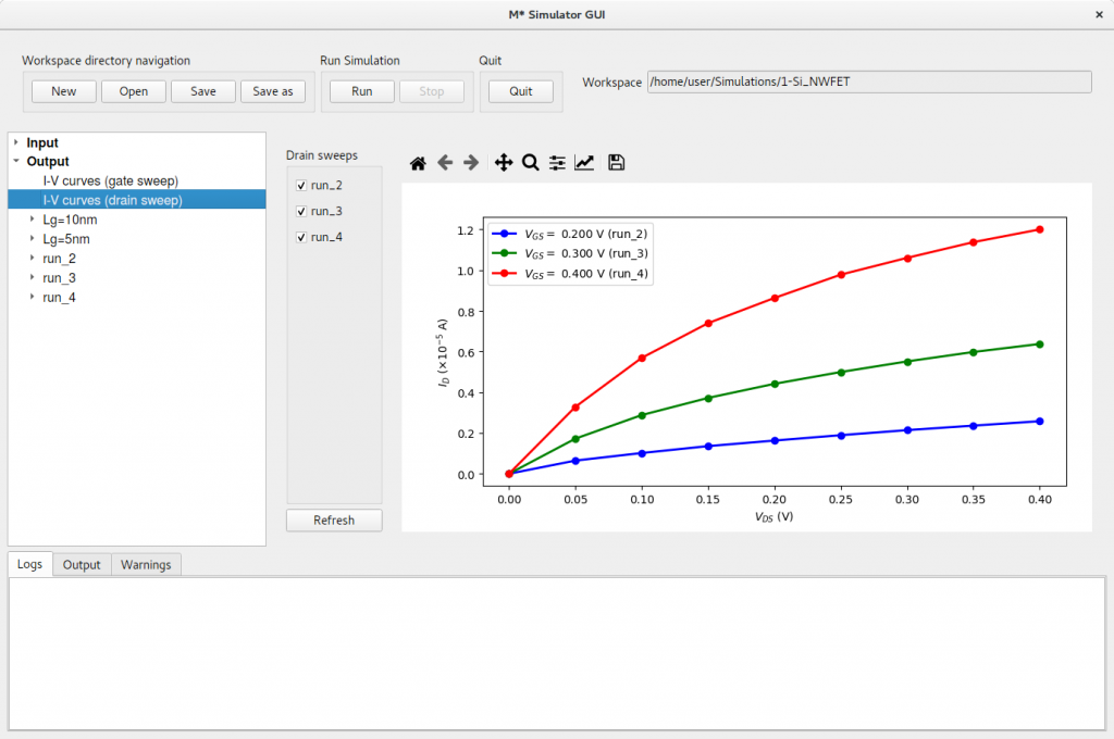
Press the Run button to begin the simulation. Upon completion, results will be available at Output->run_2 and corresponding data will be saved to a subdirectory named run_2 within your workspace directory. Additionally, a new item will be listed under Output labelled I-V curves (drain sweep); select it to display a plot of the device’s ID-VDS characteristics, as shown in figure 20.
Figure 20:The I-V curves (drain sweep) panel allows visualising ID-VDS characteristics.
To finalise this first tutorial, we shall illustrate how to visualise a family of drain curves using simulations performed at three different gate voltages: compute the two additional curves by increasing the value of Gate voltage to 0.3 V in the Input->Control panel and clicking Run; once this simulation has completed, perform one last simulation with a value of Gate voltage of 0.4 V. This process will generate run_3 and run_4, which will be listed in the left pane’s Output section. Select Output->I-V curves (drain sweep) now to visualise the results of the last three simulations in a single plot, as shown in figure 21. You may use the tickboxes shown left of the plot to select which curves you wish to plot and click the Refresh button to update the plot.
Figure 21:The I-V curves (drain sweep) panel allows comparing ID-VDS characteristics from separate runs.
")