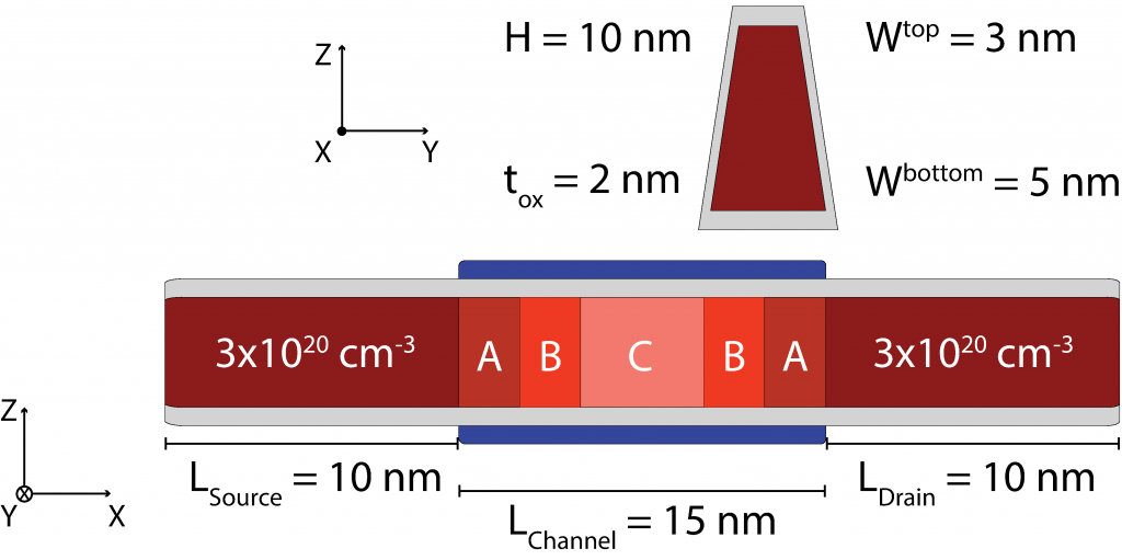
Figure 1:Ge FinFET: Schematic showing the device geometry. Red represents germanium, gray represents a low-κ dielectric, green a high-κ dielectric, yellow represents a silicon substrate, and blue the gate electrode. Regions in different shades of red represent variations in doping along the transport axis. The device is divided into several regions labelled A-D in order to describe dopant diffusion.
In this tutorial we describe how to use M* to simulate a germanium fin field-effect-transistor (FinFET) in a tri-gate configuration using the UMS mode-space method. The device is comprised of a Ge 〈100〉 fin with constant trapezoidal cross-section along the transport direction with a height of 10 nm, a width of 5 nm at the base of the fin, and a width of 3 nm at the top of the fin. Figure 1 shows a schematic of the device geometry and doping profile.
The device is divided into 7 regions in which we target varying carrier densities in order to model dopant diffusion into the channel: regions labelled A in the figure are doped to target a carrier concentration of 1 × 1020 cm-3, regions labelled B to 5 × 1019 cm-3, regions labelled C to 1 × 1018 cm-3, and region D to 1 × 1015 cm-3.
In order to prepare the input files for simulating such a device, launch the M* GUI and populate the three input panels as follows:
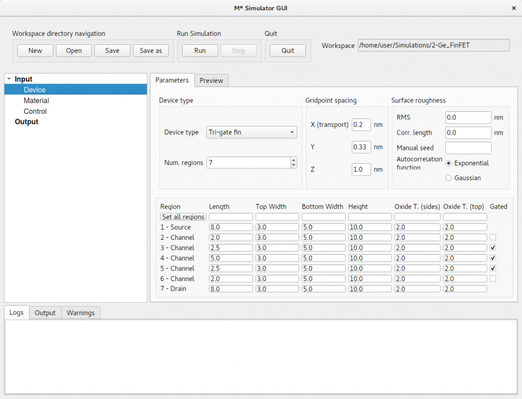
Device select Tri-gate fin device type from the dropdown menu, set the number of regions to 7, and fill out the length of each region according to figure 1 and as shown in figure 2 below. Since this device’s cross-sectional geometry is homogeneous, you may specify the corresponding fields for all regions at once by typing in values in the first row and clicking Set all regions. Set regions 3, 4, and 5 as Gated. Finally, set the Gridpoint spacing parameters to 0.2 nm × 0.33 nm × 1.0 nm to reduce simulation time. Before continuing, check the Preview tab to visualise your input geometry
Figure 2: In the Device panel, set the device type to Tri-gate fin with 7 regions and dimensions shown above. Make sure only regions 3 – 5 are Gated. Increase the gridpoint spacing to reduce simulation time.
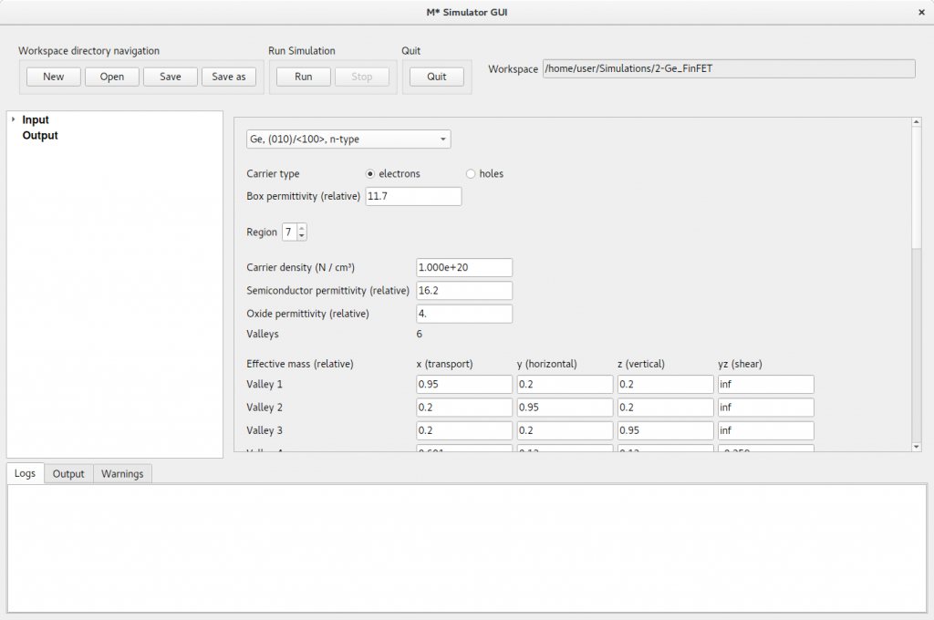
Material set the material to Ge, (010)/〈100〉, n-type to set the semiconductor properties across the whole device. Cycle through regions 1 – 7 and set target carrier densities as described above for regions labelled A – D:
A: 1 × 1020 cm-3; εoxr = 4
B: 5 × 1019 cm-3; εoxr = 4
C: 1 × 1018 cm-3; εoxr = 20
D: 1 × 1015 cm-3; εoxr = 20
Additionally, set the oxide permittivity to εoxr = 4 to describe a low-κ dielectric covering non-gated regions, and a value εoxr =20 in regions 3 – 5 to simulate a high-κ oxide in gated regions. Set the buried oxide (BOX) permittivity to that of silicon (i.e. εboxr = 11.7) to simulate a device based on the aspect-ratio-trapping (ART) heteroepitaxy technique.
Figure 3: In the Material panel, cycle through regions to set the material properties discussed in the text above.
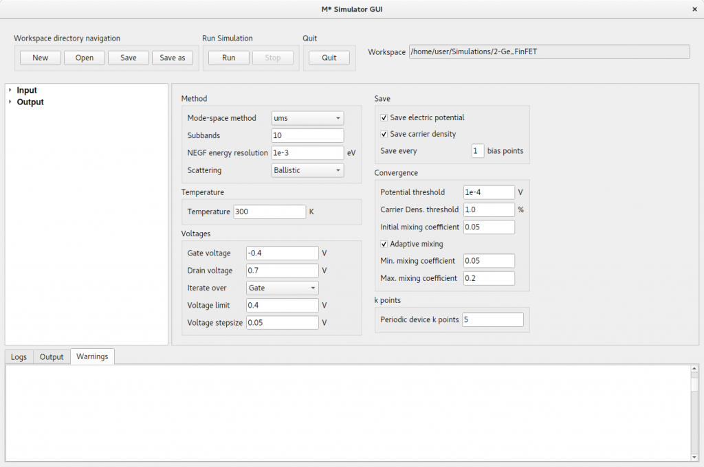
Control set the mode-space method to UMS to explicitly solve the electronic structure at each slice along the transport direction for every iteration. Increase the number of subbands per valley to 10: devices with larger cross-sectional dimensions require larger values since weaker confinement effects result in smaller energy spacing between subbands. Set a gate voltage range of [-0.4,0.40] V by specifying those values for the Gate voltage and Voltage limit fields. Specify Save and Convergence variables as shown in figure 4 below
Figure 4:In the Control panel, select the mode-space method to UMS and set the number of subbands to 10. Fill out the rest of the fields with values shown.
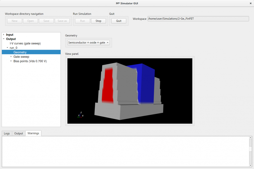
Once you have entered and checked values, press the Run button to begin the simulation. After the first bias point has converged, you will see the first set of output data available under Output->run_0. Selecting Geometry brings up a 3D render. Note that although asymmetries can be observed in the semiconductor (red) – oxide (gray) interface as a result of the method employed for visualisation; the geometry grid employed in the simulation may not contain any asymmetries that could influence simulation results.
Figure 5:Geometry of the simulated Ge FinFET. Asymmetries observed in the semiconductor-oxide interface are a visualisation artifact and not a feature of the grid employed in the simulation.
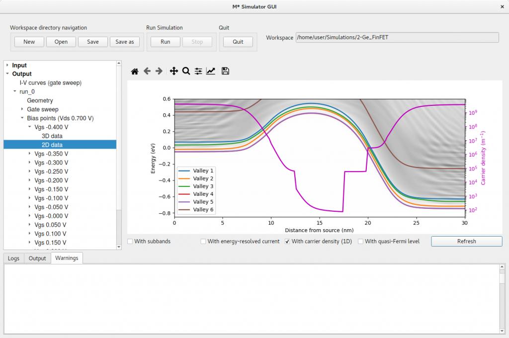
Once the simulation has completed, you may visualise all quantities discussed in the previous tutorial such as ID-VGS characteristics, subthreshold swing vs. gate voltage, etc. To plot the simulated dopant distribution plot the 2D data associated with an OFF state and include the 1D carrier density profile by activating the corresponding tickbox and clicking Refresh, as shown in figure 6. Note the carrier density discontinuities occurring at the boundaries across regions.
Figure 6:Local density of states and 1D carrier density profile for an OFF state.
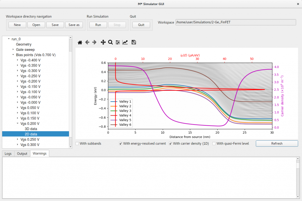
Select the 2D data corresponding to an ON state to plot the associated local density of states and each valley’s first subband; overlay both energy-resolved current and 1D carrier density profile to generate a figure similar to that shown in figure 7. Note discontinuities in the 1D carrier density profile imposed by the doping profile have now been washed out by the larger carrier densities associated with ON states. From the energy-resolved current (red curve) and first subbands for each valley we can observe that Valley 6 does not participate in transport and could be safely ignored in the simulation without altering results. This corresponds to the Γ valley, whose low effective mass (0.041) results in a large impact of quantum confinement effects and thus a significant shift towards higher energies, rendering it irrelevant for the transport properties of this nanoscale device.
Figure 7:Local density of states, energy-resolved current, and 1D carrier density profile for an ON state.
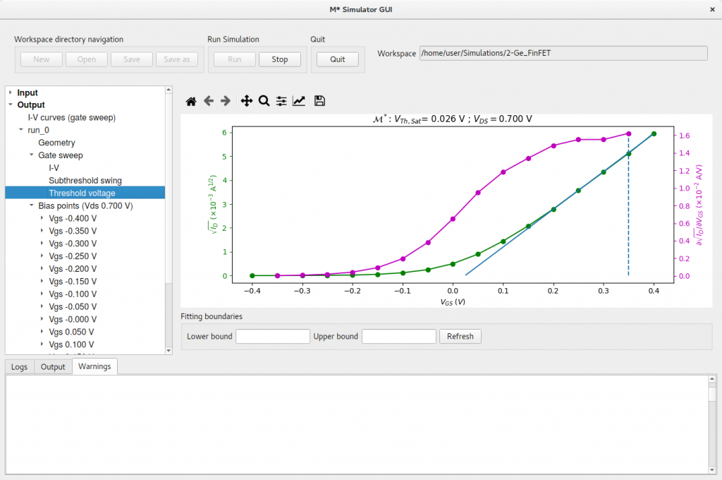
Let us now inspect the shape of the electric potential and carrier density as the device turns ON; go into Output->run_0->Gate sweep->Threshold voltage to find an appropriate bias point to investigate.
Figure 8: Threshold voltage extraction using the linear extrapolation method for saturation region of operation (i.e. large VDS).
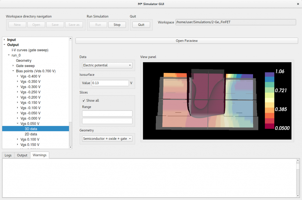
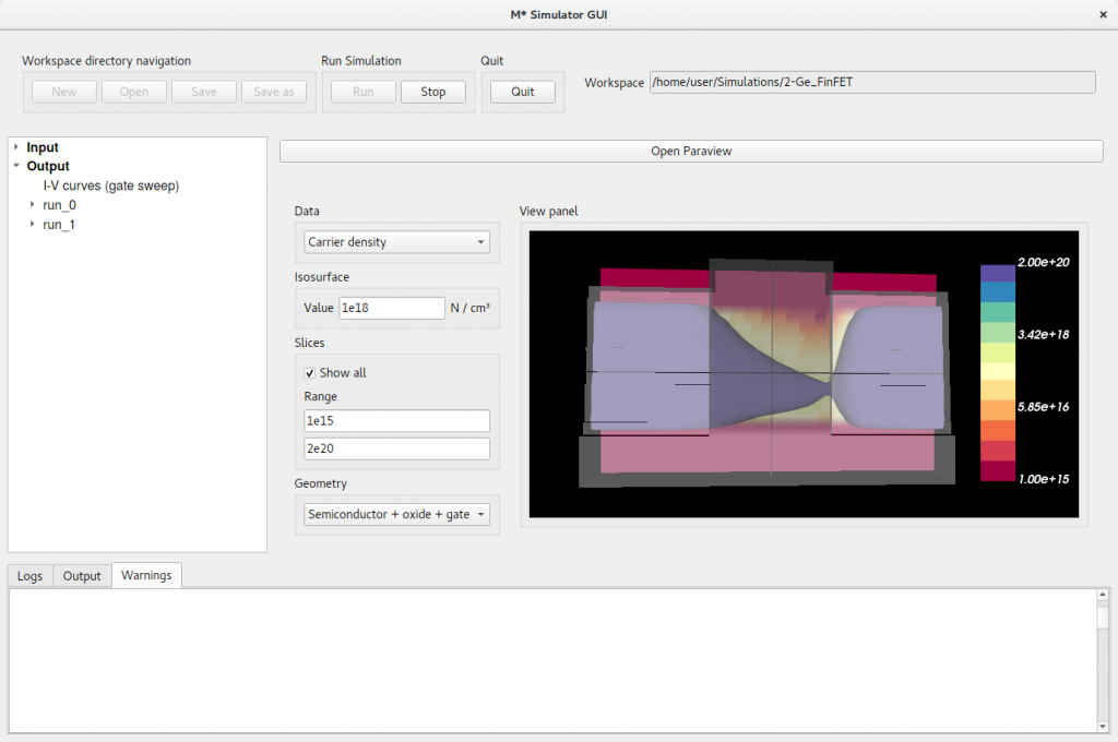
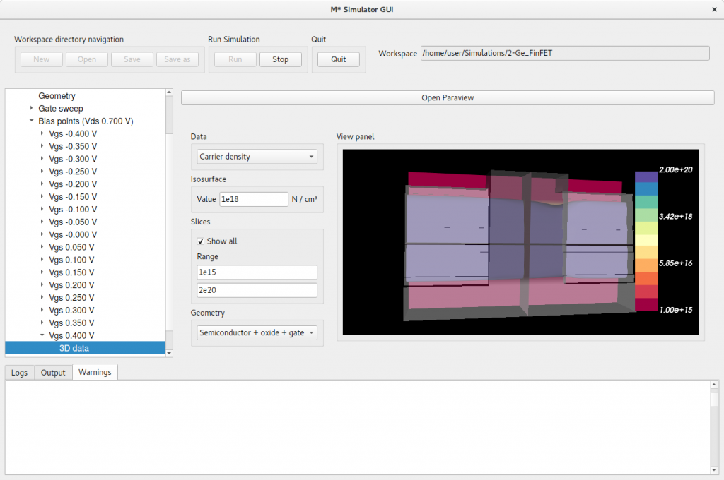
As shown in figure 7, a value of VTh,Sat close to 0.050 V is found for this device. Visualise the 3D data output for VGS = 0.050 V to inspect the electric potential and carrier density as the device turns on: asymmetries along the transport and height directions can be observed in both quantities as a result of the applied drain-source bias and trapezoidal cross-section, respectively. Note how the isosurfaces plotted in figures 8 and 9 reveal charge carriers begin to flow from the bottom half of the fin as the device turns ON. You may confirm carrier density increases near the top of the fin for larger values of VGS by inspecting the 3D carrier density for higher ON states, as shown in figure 10.
Figure 9:Electric potential around VGS = VTh,Sat.Figure 10:Carrier density around VGS = VTh,Sat. Shown isosurface corresponds to a carrier density of 1018 cm-3.Figure 11:Carrier density when the device is in saturation region. Shown isosurface corresponds to a carrier density of 1018 cm-3.
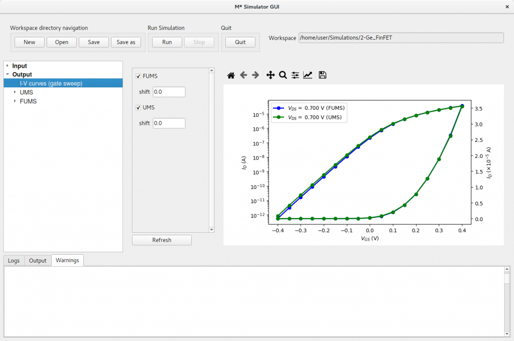
To finish this tutorial, we explore the effect of employing the fast uncoupled-mode space approximation for simulating this device’s transfer characteristics. Select Input->Control in the left pane and change the mode-space method to FUMS while maintaining the same values for all other simulation parameters; click Run to begin the simulation. This simulation should be significantly faster. Once completed, you will find the corresponding output data listed in Output->run_1. Select Output->I-V curves (gate sweep) in the left pane to show a comparison of ID-VGS curves simulated with UMS and FUMS, as shown in figure 11. Note how slight differences can be observed in the semilogarithmic plot only for OFF states, while differences are only noticeable in the linear scale plot for ON states. This is a consequence of the fact that differences in computed current values differ significantly more in OFF states (up to ≈ 35 %) than in ON states (up to ≈ 10 %). You can confirm differences in other computed quantities such as subthreshold slope and threshold voltage are negligible, making FUMS an attractive alternative for simulating certain properties of small devices with by yielding satisfactory results at a lower computational cost.
Figure 12:Transfer characteristics computed with UMS (run_0) and FUMS (run_1).
")