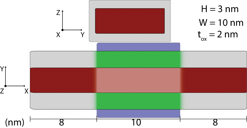
Figure 1:In0.53Ga0.47As nanosheet FET: Schematic showing the device geometry. Red represents In0.53Ga0.47As, gray represents a low-κ oxide, green a high-κ oxide, and blue the gate electrode.
In this tutorial we simulate a nanosheet-based device comprised of a III-V channel material. Nanosheet device types allow simulating the properties of quasi-planar devices where effects due to the semiconductor’s finite width are explicitly treated. To set up this simulation start a new M* workspace and set input parameters as:
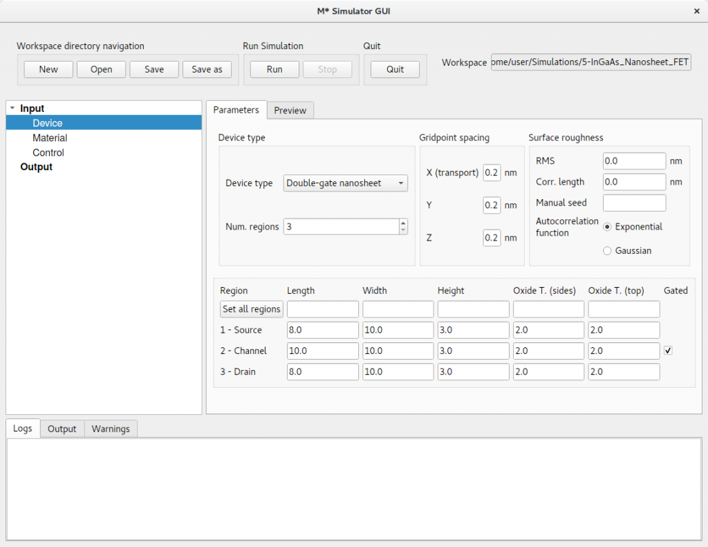
Device select Double-gate nanosheet as the device type and enter geometrical parameters in accordance with figure 1 and as shown below in figure 2. Once you have finished, check the geometry corresponds to the intended design by visualising it in the Preview tab
Figure 2:In the Device panel, specify a Double-gate nanosheet with 3 regions and dimensions shown above.
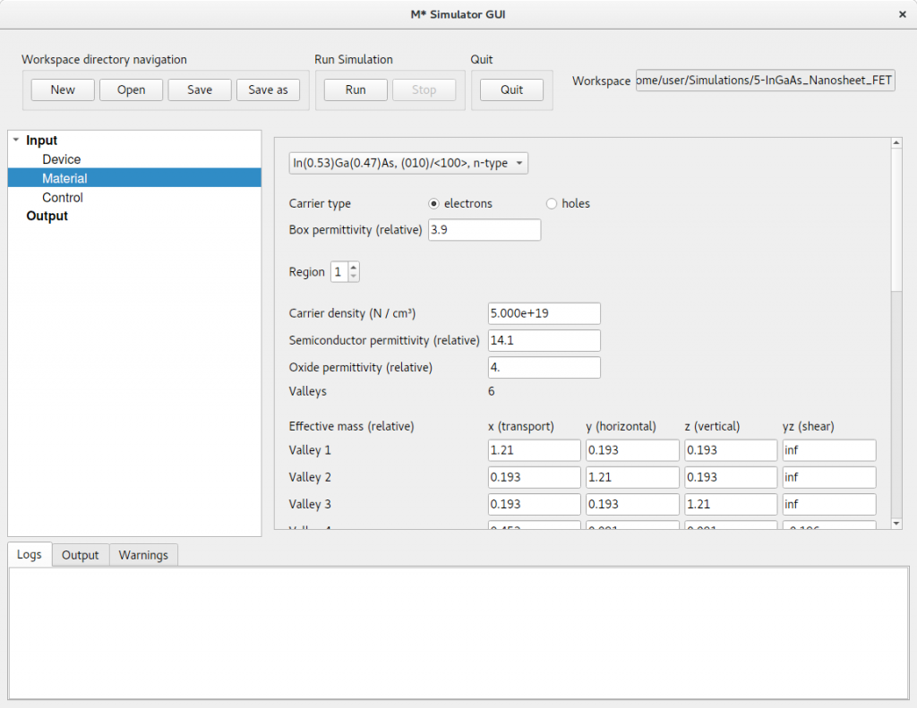
Material select In(0.53)Ga(0.47)As, (010)/〈100〉, n-type and cycle through regions to set a target carrier concentration of 5 × 1019 cm-3 in source and drain extensions (i.e. regions 1 & 3), and zero in region 3. Input an oxide relative permittivity of εr = 4.0 (low-κ oxide) in source and drain extensions, and a value εr = 20.0 (high-κ oxide) in the channel. The low-κ oxide will reduce capacitive coupling between the gate electrode and source/drain extension regions
Figure 3:In the Material panel, specify a carrier concentration of 5 × 1019 cm-3 and an oxide relative permittivity εr = 4.0 in both source and drain extensions, and a zero carrier concentration and &epsilonr = 20.0 in the channel.
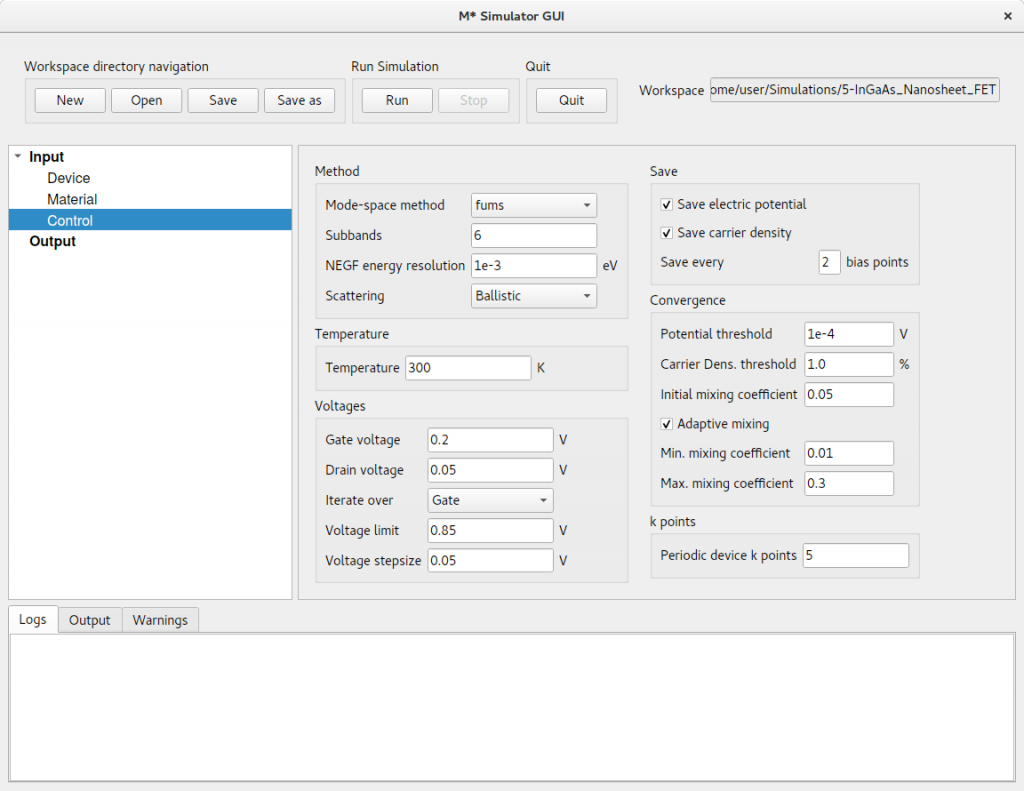
Control select fast uncoupled-mode space (FUMS) as the mode-space method, and subbands to 6. Set a gate voltage sweep covering the [0.0,0.85] V range in steps of 0.05 V, and a drain voltage of 0.05 V. Enable saving electric potentials and carrier densities and set Save every [2] bias points to reduce disk space usage. Set the same convergence parameters as in previous tutorials and shown in figure 4
Figure 4:In the Control panel, enter parameter values shown in the figure and discussed in the text.
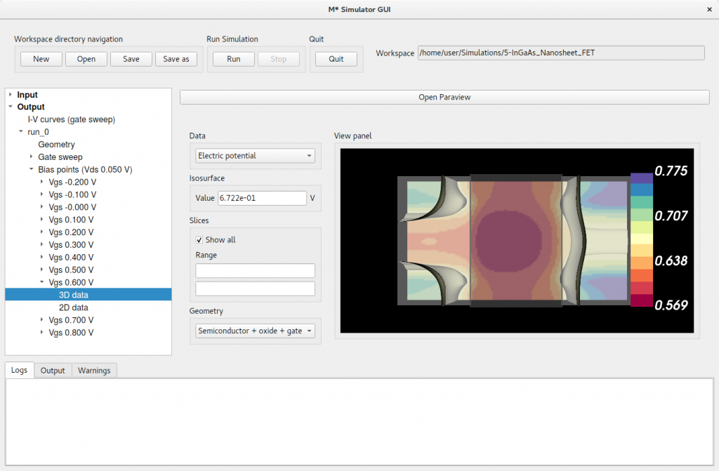
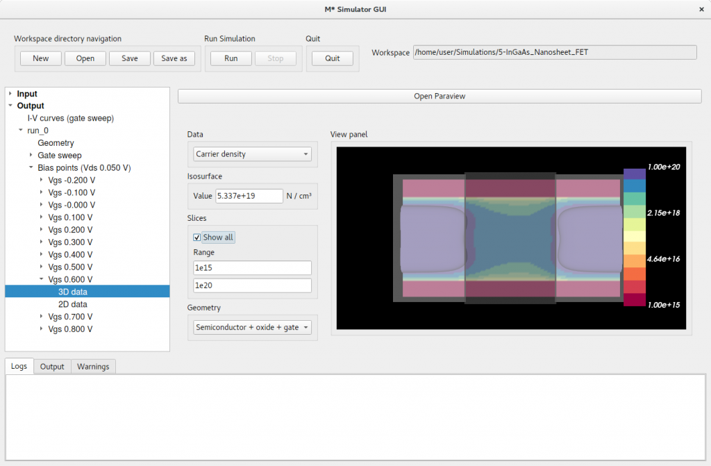
Click Run to begin the simulation. Once completed, you may visualise the 3D quantities to observe the influence of the device’s finite width on both electric potential and carrier density, as shown in figures 5 and 6 for an ON state.
Figure 5:Electric potential at VGS = 0.6 V (ON state).Figure 6:Carrier density at VGS = 0.6 V (ON state). Note the range for the contour plot has been manually set to [1015,1020] cm-3
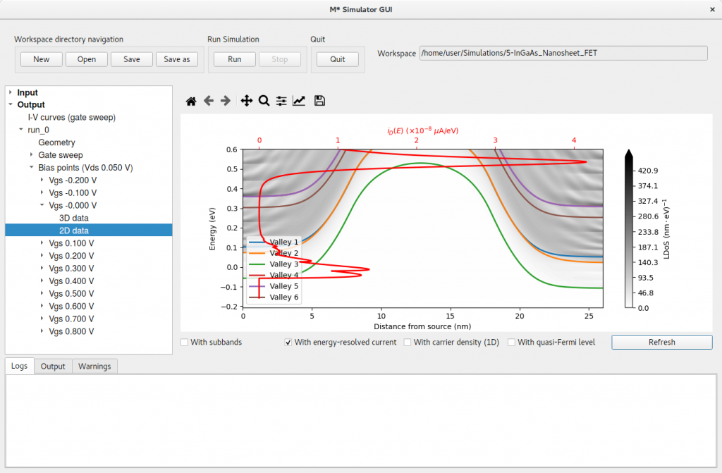
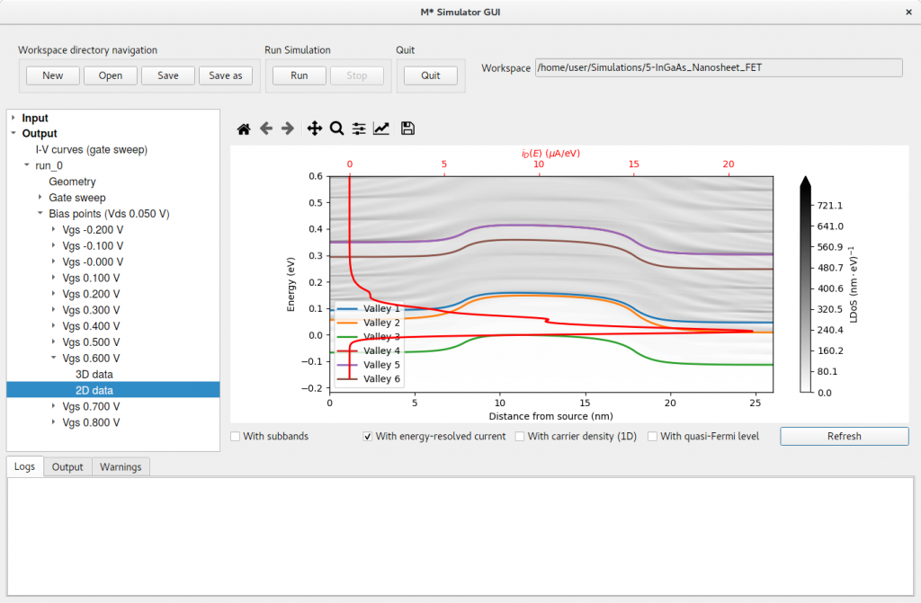
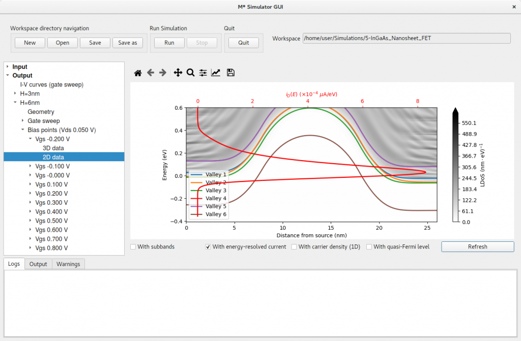
Next, inspect 2D data for various bias point to visualise plots similar to figures 7 and 8 (OFF and ON states, respectively). We can observe that the properties of this device are dominated by valleys 1 – 3, corresponding to the three X valleys in In0.53Ga0.47As. The significantly lower effective masses of valleys 4 & 5 (L valleys), and valley 6 (Γ valley) along cross-sectional dimensions result in larger confinement-induced shifts to their associated subbands towards higher energies, rendering their impact on the properties of this device negligible.
Figure 7:Local density of states, lowest subband for each valley, and energy-resolved current at VGS = 0.0 V (OFF state).Figure 8:Local density of states, lowest subband for each valley, and energy-resolved current at VGS = 0.6 V (ON state).
To explore the geometrical dependence of confinement-induced energy shifts and their impact on device operation, let us simulate a similar device with a thicker channel:
Device edit the device geometry by modifying the value of Height fields with a value of 6 nm for all three regions
Control edit the gate voltage sweep range to [-0.2,0.85] V to cover more OFF states
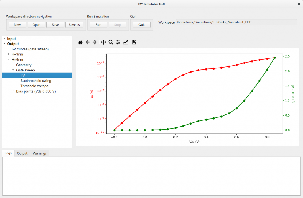
Click Run to begin the simulation. Once finished, let us make identifying both devices easier by renaming run_0 to H=3nm, and run_1 to H=6nm. We begin our analysis by visualising the corresponding I-V characteristics, shown in figure 9. Note the device appears to turn ON in two stages with a first contribution appearing for VGS > 0.2 V, and a second contribution for VGS > 0.6 V.
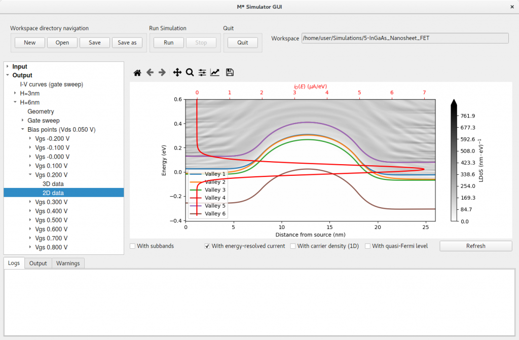
Plotting 2D data for VGS = 0.2 V illustrates device operation around the point where the first contribution begins. Figure 10 shows the device begins turning ON when the bottom subband in valley 6 (Γ valley) comes in alignment with the source’s Fermi level. Note that valley 6 is lower in energy in this device and the first subband in all six valleys lie at energies below 0.2 eV above the source Fermi level, making them all relevant to this device’s properties. The reduced confinement in this structure with larger cross-sectional dimensions has dramatically changed the electronic structure compared to the device based on a nanosheet with 3 nm height.
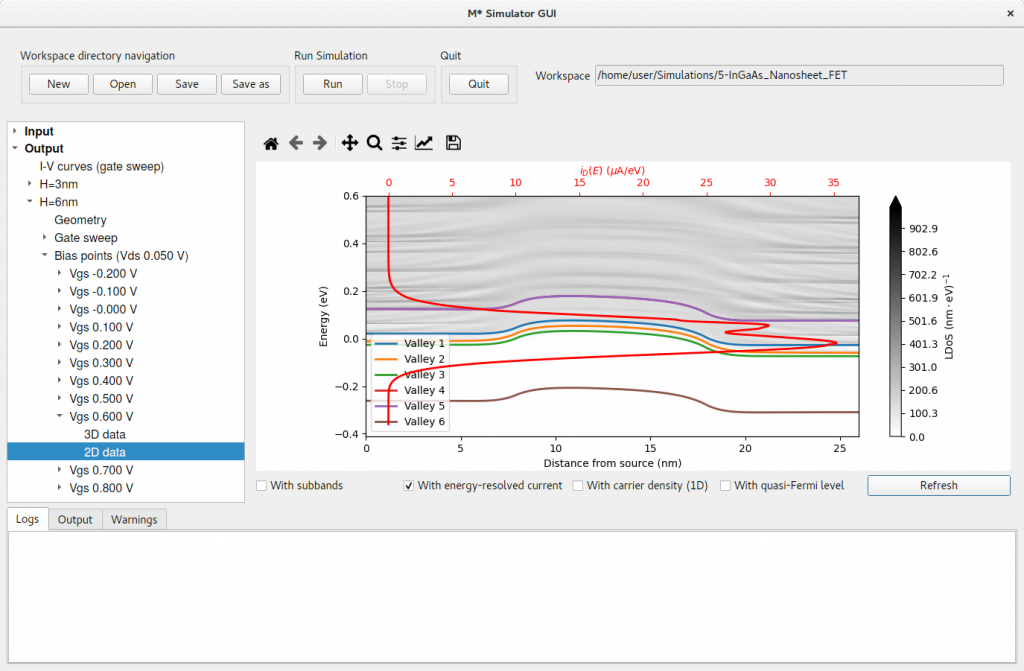
Figure 11 shows the 2D data panel for VGS = 0.6 V. The energy-resolved current reveals that the second contribution observed in the I-V characteristics occurs for gate bias values high enough such that valleys 1 – 3 (i.e. X valleys) in the channel are aligned with the Fermi level at the source.
Figure 9:ID – VGS characteristics for device with 6 nm height.Figure 10:Local density of states, lowest subband for each valley, and energy-resolved current for the thicker device at VGS = 0.2 V (ON state).Figure 11:Local density of states, lowest subband for each valley, and energy-resolved current for the thicker device at VGS = 0.6 V (ON state).
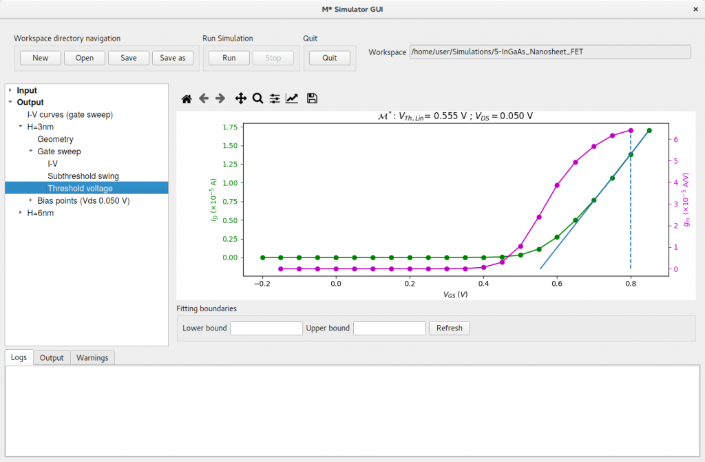
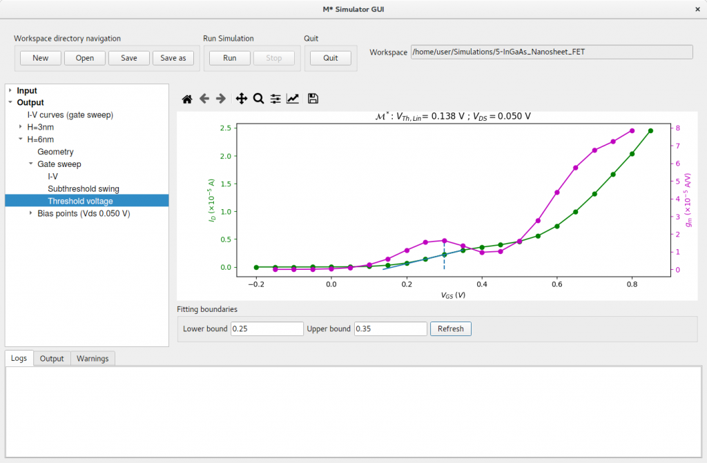
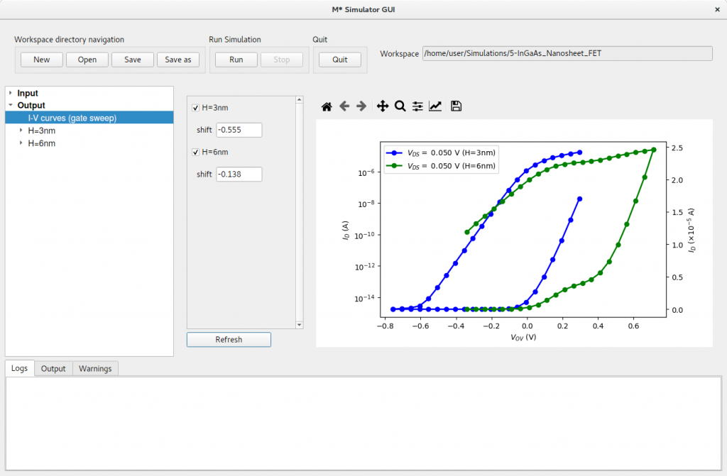
In order to compare both devices’ in a more meaningful manner, let us shift their I-V characteristics by their respective threshold voltages. Extracting the threshold voltage of the device with H = 3 nm should be straightforward, resulting in a value of VTh,Lin = 0.555 V (figure 12). Attempting to obtain a threshold voltage value for the thicker device requires some tweaking: by default, M* attempts a fit around the point of maximum conductance (gm, right axis in figure 13). Manually enter lower and upper bounds of [0.25,0.35] V and click Refresh to recalculate a fit around the first conductivity maximum to obtain a more appropriate value of VTh,Lin = 0.138 V, as shown in figure 13. Finally, click on Output->I-V curves (gate sweep) and enter shift values corresponding to each device’s -VTh,Lin (with opposite sign) to align their threshold voltage with VG = 0 V. Click Refresh to generate a plot similar to figure 14.
Figure 12:Threshold voltage extraction for the device based on a nanosheet with a height of 3 nm.Figure 13:Threshold voltage extraction for the device based on a nanosheet with a height of 6 nm. Note that a manual range has been specified for the fit.Figure 14:Comparison of both nanosheet device’s transfer characteristics. Curves have been shifted such that their threshold voltage aligns with VG = 0 V.
Figure 14 shows that the thicker device exhibits a larger subthreshold swing, and a lower ON current at the same overdrive voltage VOV = VGS-VTh. (Note: The horizontal axis’ label has been manually set to VOV using the toolbar at the top of the plot.) Comparing subthreshold swing values computed for both devices quantifies observed differences with the thicker device surpassing 100 mV/dec, while the thinner device exhibits values below 70 mV/dec. Inspecting 2D data for the thicker device’s OFF states reveals the main reason behind this significantly different behaviour: OFF currents are dominated by source-to-drain current (e.g. figure 15) whereas the thinner device’s OFF currents are dominated by thermionic emission (e.g. figure 7). This contrast is largely a consequence of the Γ valley’s lower effective mass value along the transport direction.
Figure 15:Local density of states, lowest subband for each valley, and energy-resolved current for the thicker device at VGS = -0.2 V (OFF state).
")