In this last test case we cover the inclusion of two types of scattering into M* simulations: acoustic phonon scattering, and surface roughness scattering. We will employ a silicon nanowire FET structure simulated with a channel length of 10 nm.
If you have already followed the silicon nanowire FET tutorial, click Open in the M* GUI’s top pane and select the corresponding workspace’s top folder to load all associated data and append the results from this tutorial into it
If you have not yet followed the silicon nanowire FET tutorial, click Open in the M* GUI’s top pane and select an empty folder. See our tutorial on a SiNW FET for instructions on how to set up the input parameters for a ballistic simulation
Acoustic phonon scattering
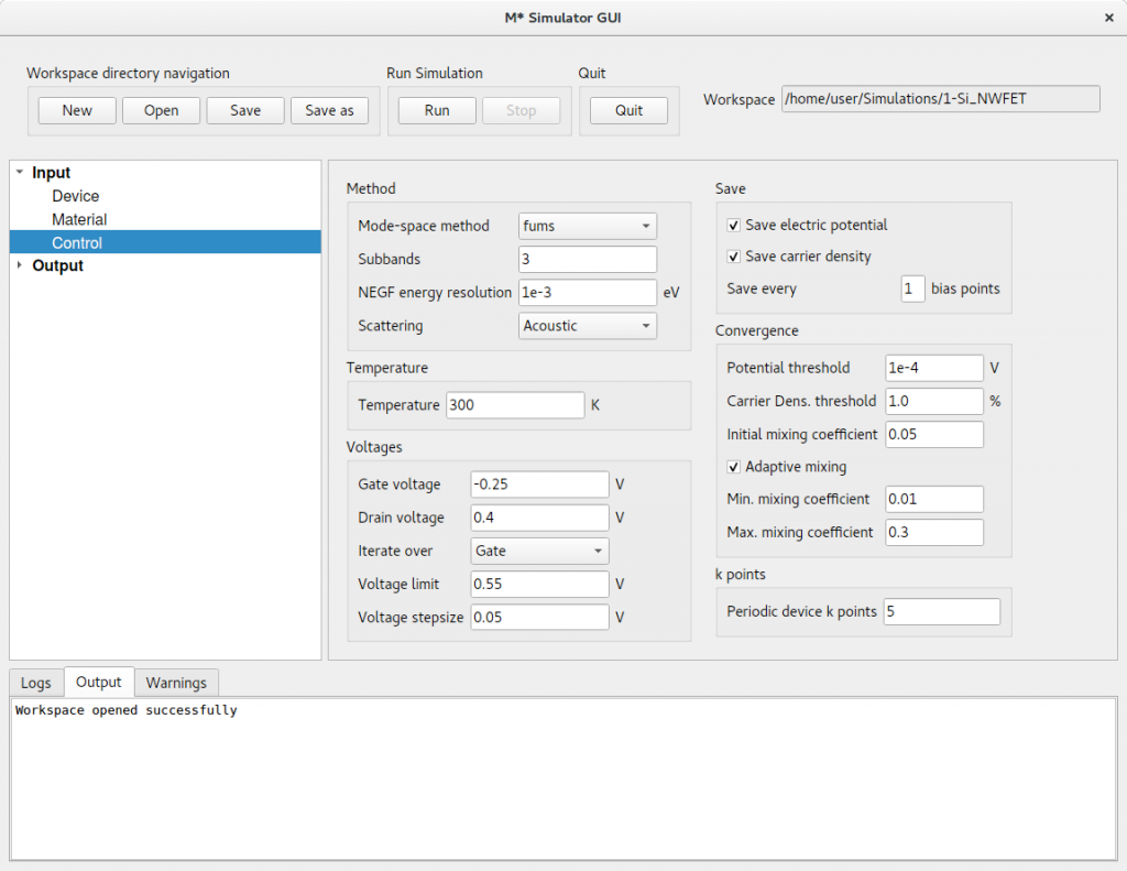
Using input parameters employed for the first simulation described in our SiNW FET tutorial as a starting point, click on Input->Control and set Scattering: Acoustic, as shown below. Click Run to begin the simulation.
Figure 1:In the Control panel, select Acoustic from the Scattering dropdown menu.
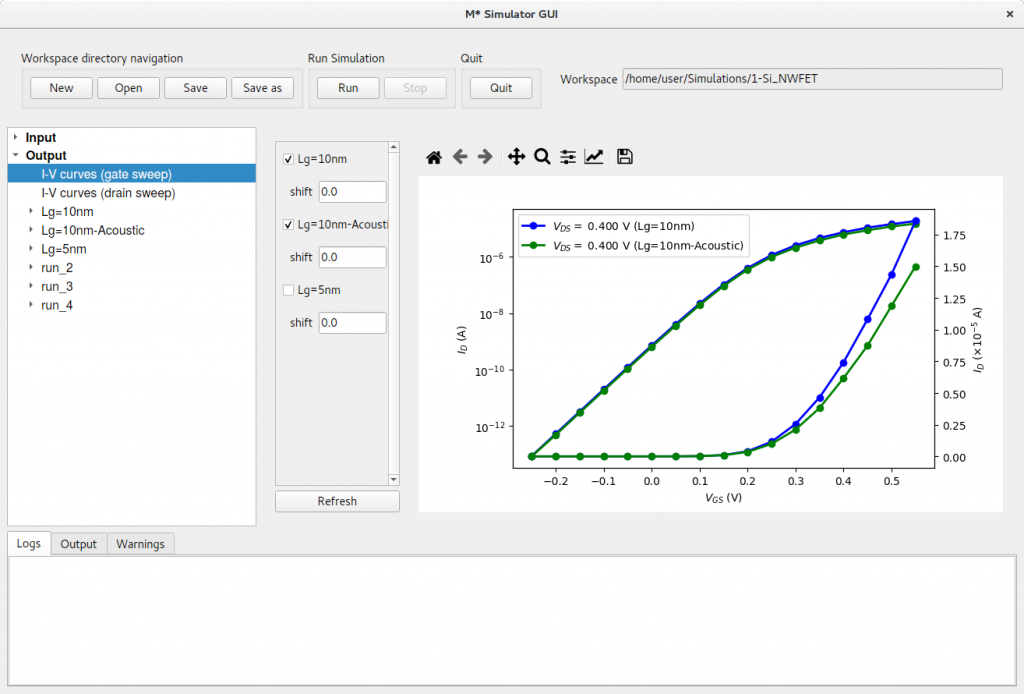
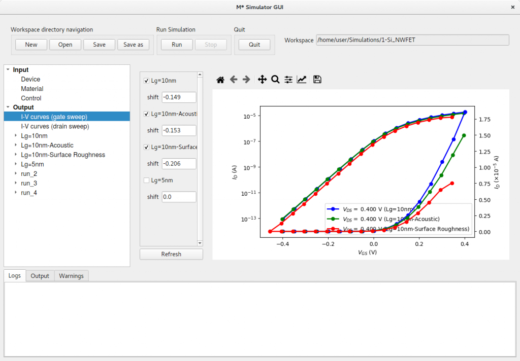
Once finished, you can compare the effects of including acoustic phonon scattering in your simulation. In Output->I-V curves (gate sweep), compare transfer characteristics by selecting only this most recent simulation and its corresponding ballistic equivalent from the list on the left. Figure 2 shows the resulting plot; although both curves exhibit the same general characteristics and subthreshold slope, the simulation including scattering from acoustic phonons shows lower current. Inspection of the data shows scattering lowers the drain current, with larger drops observed for ON states.
Figure 2:Transfer characteristics of silicon nanowire FET with acoustic phonon scattering, and in the ballistic approximation.
Surface roughness scattering
To include the scattering induced by surface roughness in your simulation, M* explicitly generates a surface roughness profile along your device. This approach is preferred to employing ensemble averages for short-channel devices where lengths may not allow for statistical averages to hold; furthermore, this methodology allows studying variations between different individual devices in more detail.
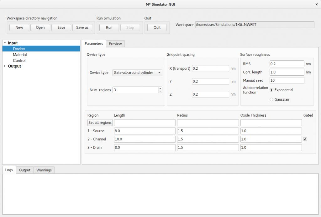
To enable roughness in your device geometry, click on Input->Device and find the Surface roughness variables at the top right. As shown in figure 3, we shall input an RMS amplitude of 0.2 nm, a correlation length of 1.0 nm and choose an exponential autocorrelation function for the generation of the profile. The Manual seed field allows some control over the random number generator employed when generating the profile; input a value of 10 to obtain the same profile studied in this tutorial or leave blank to use a seed based on your system’s clock. (Note: the geometry preview tab does not show surface roughness profiles; you may only visualise the structure including surface roughness in the Output section.)
Figure 3: In the Device panel, input variables shown above in the Surface roughness section at the top right.
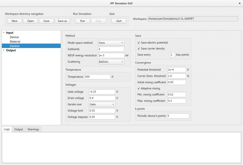
Finally, click on Input->Control and select CMS as mode-space method; cross-sectional inhomogeneities produced by the roughness profile require coupling between modes in adjacent slices to be explicitly computed. Ensure Scattering is set to ballistic in order to be able study the effects of surface roughness and acoustic scattering separately later on. Click Run when you are ready to begin the simulation.
Figure 4:In the Control panel, select the CMS mode-space method and ballistic scattering.
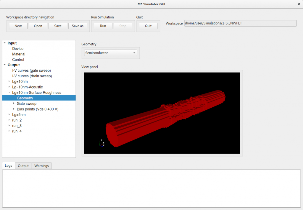
You may visualise the geometry output once a first bias point has converged (figure 5). Note only the device channel exhibits a roughness profile. In general, surface roughness profiles are generated for all device regions except source and drain extensions (i.e. first and last geometry regions).
Figure 5:Geometry (semiconductor only) of simulated device including surface roughness profile in the channel.
Once your simulation has completed, you may include ID – VGS characteristics in the comparison performed in the previous section. Compare transfer characteristics using Output->I-V curves (gate sweep) by selecting both curves plotted in figure 2 and the surface roughness curve. Figure 6 shows a comparison between the three cases: ballistic, acoustic phonon scattering, and surface roughness scattering; it is clear that scattering induced by the surface roughness profile is larger than that induced by acoustic phonon modes. Note that curves have been shifted by their threshold voltage in order to compare them in a meaningful way, as illustrated in the previous tutorial.
Figure 6:Shifting curves to make threshold voltages coincide allows meaningful comparisons. The simulated surface roughness profile degrades current more than acoustic phonon scattering in the smooth device.
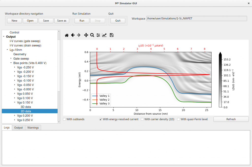
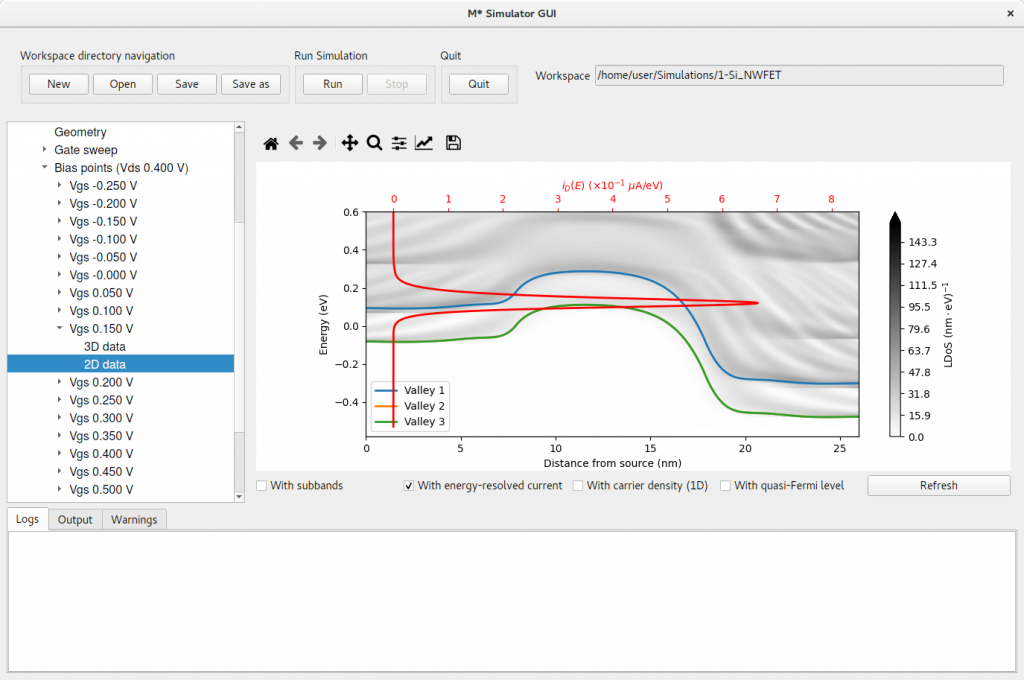
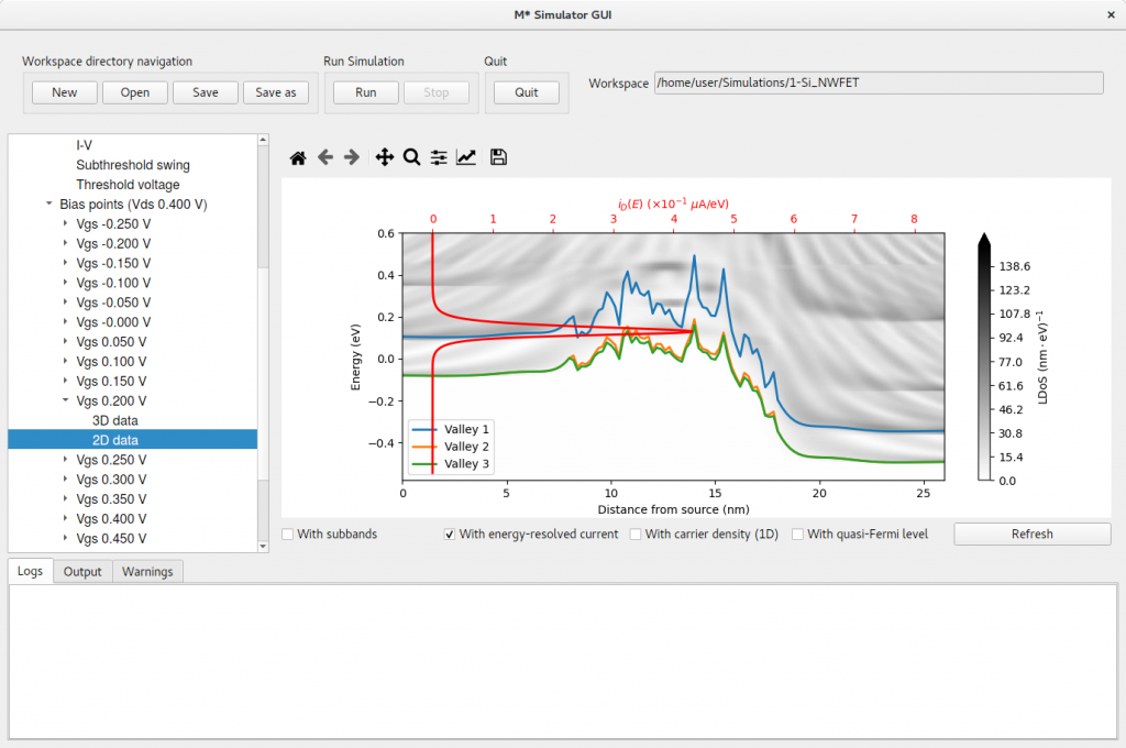
To finalise this tutorial, let us investigate the effects of both types of scattering on carrier density throughout the device, energy-resolved current, and local density of states. Figures 7, 8, and 9 show the corresponding 2D data plots near their threshold voltages. Note limits on energy-resolved horizontal axes have been edited using each plot’s toolbar in order to facilitate comparisons.
Acoustic phonon scattering reduces oscillations and resonances in the LDoS, resulting in a smoothed contour plot when compared to the ballistic case. Back scattering of carriers by phonon modes results in a reduction of carrier density in the channel, as well as a reduced energy-resolved current
Surface roughness scattering reduces oscillations and resonances in the LDoS, similar to the acoustic phonon scattering case. Variations in subband energies across different slices result in channel regions with localised states, shown as darker regions in the LDoS plot; their impact can also be observed as fluctuations in the carrier density along the channel not present in the smooth device. Local barriers induced by subband energy variations impose tunnelling barriers on carriers travelling through certain regions of the channel and reduce the magnitude of the energy-resolved current.
Figure 7:Local density of states and energy-resolved current for the ballistic simulation near its threshold voltage.Figure 8:Local density of states and energy-resolved current for the simulation with acoustic phonon scattering near its threshold voltage.Figure 9:Local density of states and energy-resolved current for the simulation including surface roughness near its threshold voltage.
")