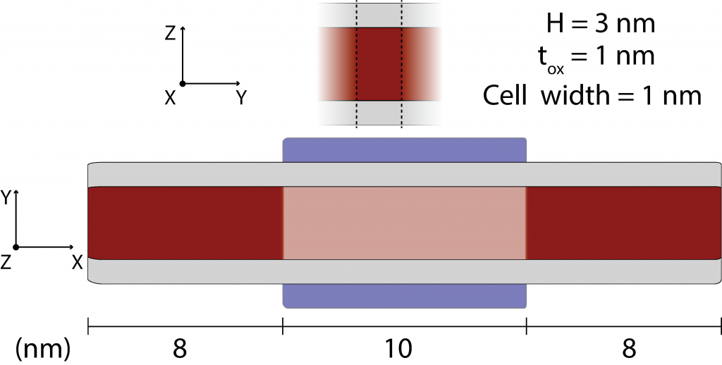
Figure 1:Si double-gate planar FET: Schematic showing the device geometry. Red represents silicon, gray represents silicon dioxide, and blue the gate electrode.
This tutorial illustrates the usage of two elements not covered in previous test cases:
Planar devices are devices whose width is large enough that we may simulate them as effectively infinitely wide by employing periodic boundary conditions. The top portion of figure 1 illustrates the device cross-section: we shall simulate a 1 nm-wide cell and employ k-point integration over quantities to compute the properties of an infinitely wide device. The bottom portion of the figure shows the device geometry along the transport direction: a double-gate ultra-thin body (UTB) geometry comprised of a 10 nm long channel and 8 nm long source and drain extensions
p-type materials we note the effective-mass formalism is widely regarded as a crude approximation to the properties of p-type devices due to strong anisotropy, non-parabolicity & bias-dependent tunnelling between heavy hole, light hole, and split-off bands relevant to transport in devices comprised of p-type materials. While M* includes parameter sets corresponding to some p-type materials, it is recommended that more sophisticated electronic structure methods are employed when attempting to accurately predict or reproduce the behaviour of real devices
To simulate the properties of this device, open the M* GUI and populate input parameters as follows:
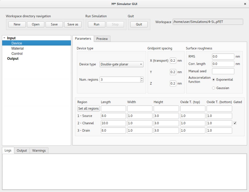
Device select Double-gate planar as the device type and enter geometrical parameters as shown below in figure 2. Once you have finished, check the geometry corresponds to the intended design by clicking on the Preview tab
Figure 2:In the Device panel, specify a Double-gate planar with 3 regions and dimensions shown above.
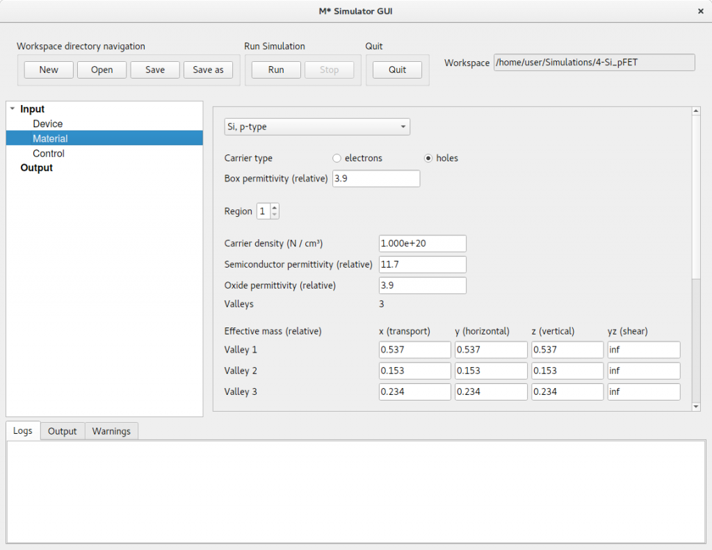
Material select Si, p-type and cycle through regions to set a target carrier concentration of 1 × 1020 cm-3 in source and drain extensions (i.e. regions 1 & 3), and zero in region 3. Leave the default oxide relative permittivity of εr = 3.9 corresponding to SiO2Figure 3: In the Material panel, specify a dopant concentration of 1 × 1020 cm-3 in both source and drain extensions and a value of zero for region 3.
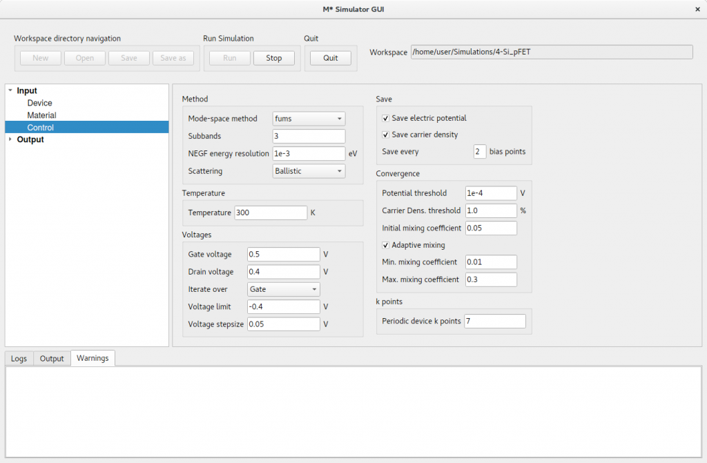
Control select fast uncoupled-mode space (FUMS) as the mode-space method, as is appropriate for devices with such small cross-sectional dimensions, and subbands to 3; note that in devices employing periodic boundary conditions and k-point sampling, this corresponds to using 3 subbands per valley and per k-point. Set a gate voltage sweep covering the [0.5,-0.4] V range in steps of 0.05 V, and a drain voltage of 0.4 V. Enable saving electric potentials and carrier densities and set Save every [2] bias points to reduce disk space usage as saving data for every other bias point should provide enough data to study this device. Set the same convergence parameters as in previous tutorials and shown in figure 4. Finally, we need to enter the amount of k-points along the width direction to incorporate periodicity into our simulation. Set Periodic device k points to 7 to perform a first run
Figure 4: In the Control panel, enter parameter values shown in the figure and discussed in the text.
Click Run to begin the simulation. Once it has completed, you may visualise output data in the same way as covered in previous tutorials.
K-point Sampling
Let us now explore the impact of varying the k-point sampling on the simulated ID – VGS characteristics of this device. After completing a first simulation performed with Periodic device k points set to 7, run two more simulations with a lower (e.g. 5) and a higher (e.g. 9) value, respectively. (Note this input parameter should always be an odd number; if an even number is specified, M* will employ the next odd number for the simulation.)
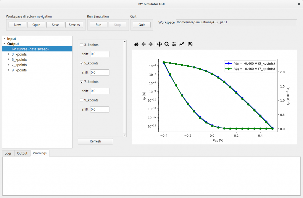
Once all simulations have completed, you may compare their transfer characteristics by clicking on Output->I-V curves (gate sweep). figure 5 shows a comparison between results obtained with 7 k-points and results obtained with 5 k-points; differences can be discerned especially in OFF states where current values vary more than 20 %.
Figure 5: Comparing the reference run (7 k-points) with a 5 k-point run results in noticeable differences, especially for OFF states.
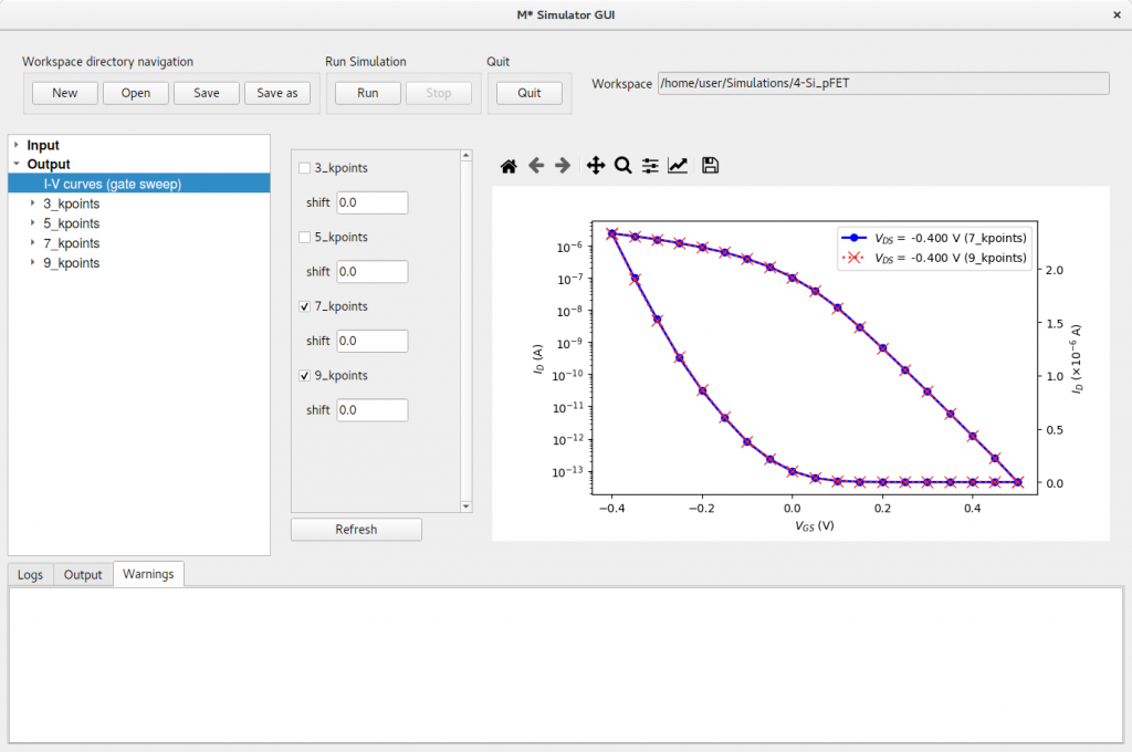
Comparing results obtained with 7 k-points and 9 k-points results in a plot where both curves fully overlap across the entire gate bias range, as shown in figure 6; the line style and symbol corresponding to the simulation with 9 k-points have been modified for clarity using the toolbar located at the top of the plot. This result indicates the simulation using 7 k-points is appropriately converged. Although wider (narrower) cell widths tend to require a lower (higher) number of k-points to reach convergence, other system properties may affect appropriate values for each system. It is highly recommended convergence with respect to this parameter is checked for each device.
Figure 6: Comparing the reference run (7 k-points) with a 9 k-point run results in curves that fully overlap across the entire gate bias range.
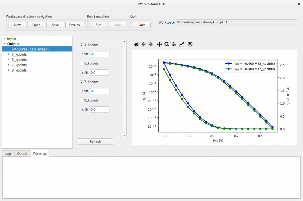
Finally, figure 7 shows a comparison between curves computed with 7 k-points, and 3 k-points. In this case differences between both curves is evident in both OFF states and ON states. Note differences in OFF states tend to be larger than in ON states, as can be observed from the semilogarithmic plot.
Figure 7: Comparing the reference run (7 k-points) with a 3 k-point run results in noticeable differences in both ON and OFF states.
")