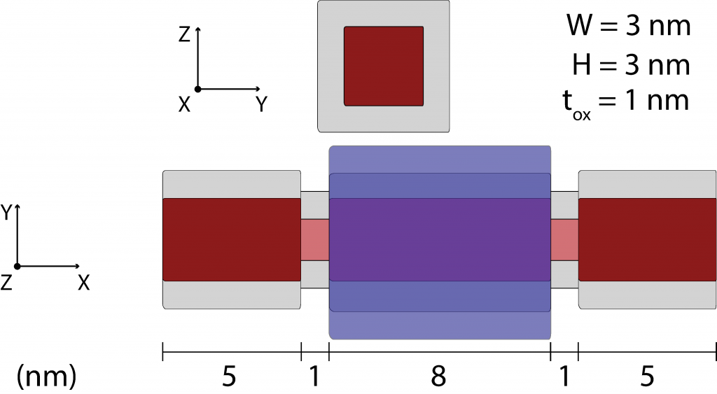
Figure 1: Schematic showing the device geometry. Red represents silicon, gray represents silicon dioxide, and blue the gate electrode.
In this tutorial we illustrate M*‘s capabilities for simulating the properties of devices whose operation inherently depends on quantum mechanical effects through a single-electron transistor design. The device is comprised of a Si nanowire with tunnelling barriers on either side of the channel realised via geometrical constrictions. To set up a simulation for this device, fill out the input panels as follows:
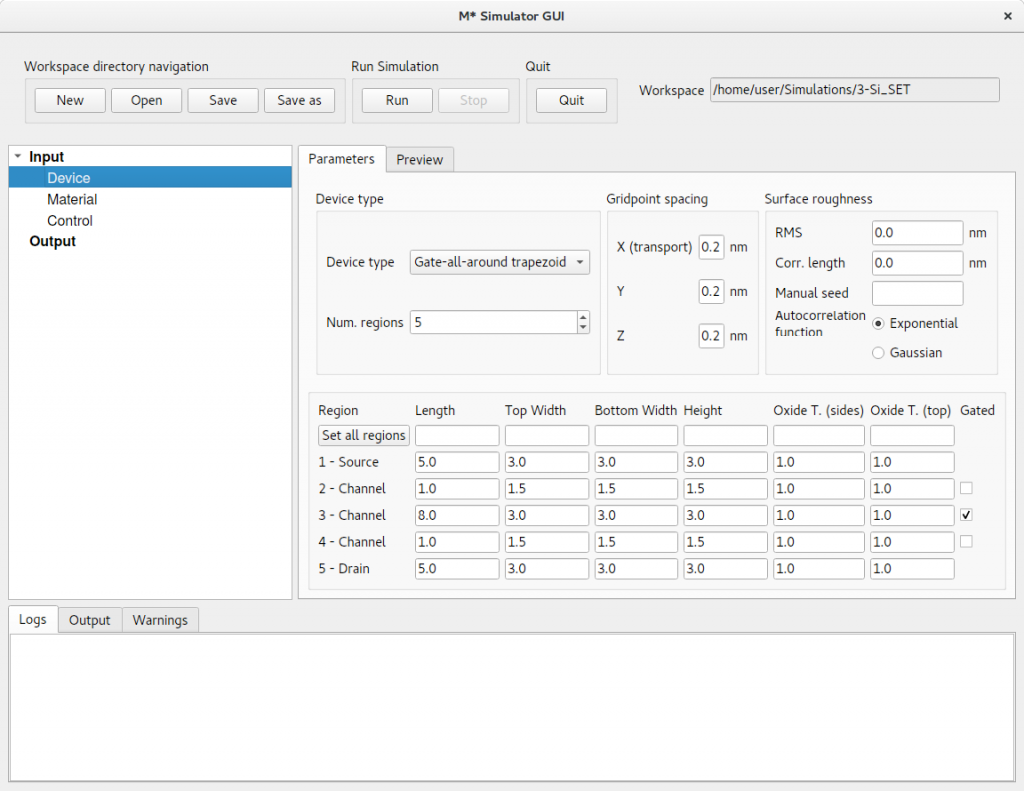
Device select Gate-all-around trapezoid as the device type and enter geometrical parameters in accordance with figure 1 and as shown below in figure 2. Note that although we shall be simulating a device with a square cross-section, this device type allows variations in width between the top and bottom portions of the geometry. Once you have finished, check the geometry corresponds to the intended design by clicking on the Preview tab
Figue 2:In the Device panel, specify a Gate-all-around trapezoid with 5 regions and dimensions shown above. Make sure only region 3 (i.e. the device channel) is Gated.
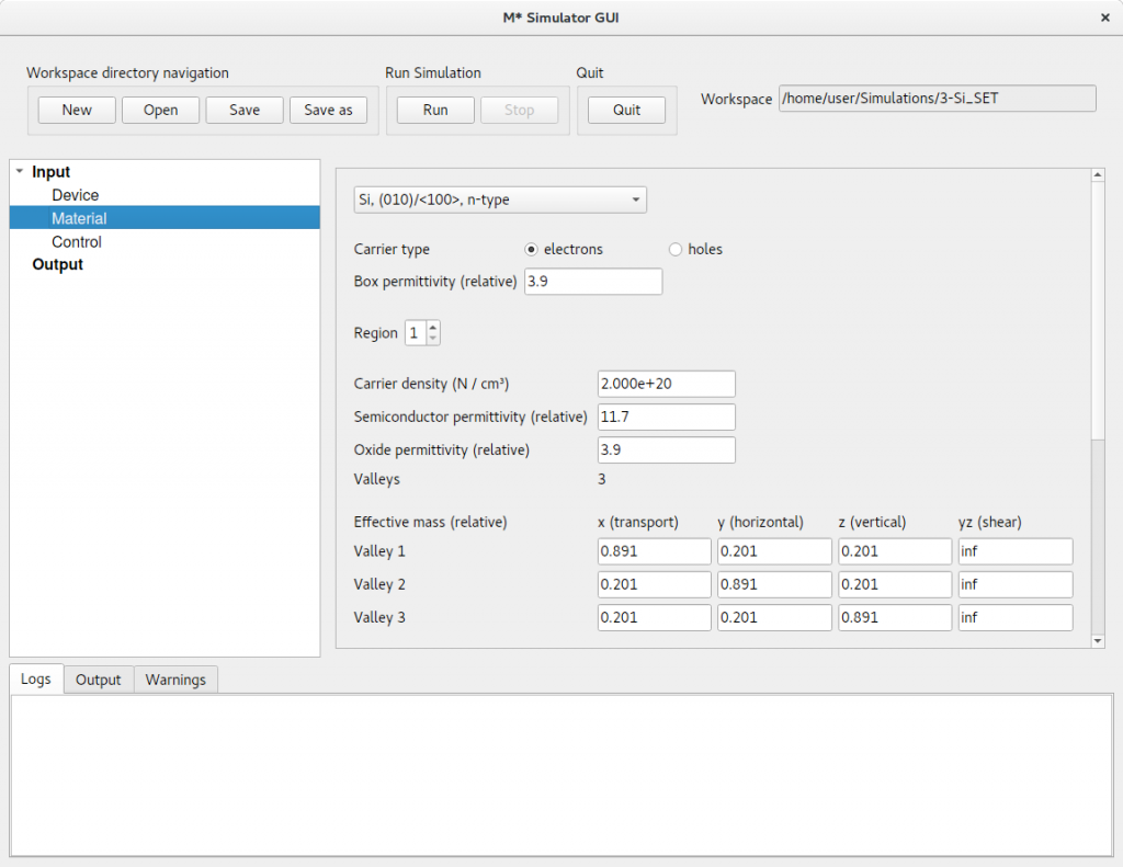
Material select Si, (010)/<100>, n-type and cycle through regions to set a target carrier concentration of 2 × 1020 cm-3 in source and drain extensions (i.e. regions 1 & 5), and zero in regions 2 – 4. Leave the default oxide relative permittivity of εr = 3.9 corresponding to SiO2Figure 3:In the Material panel, specify a dopant concentration of 2 × 1020 cm-3 in both source and drain extensions and a value of zero for all regions in between.
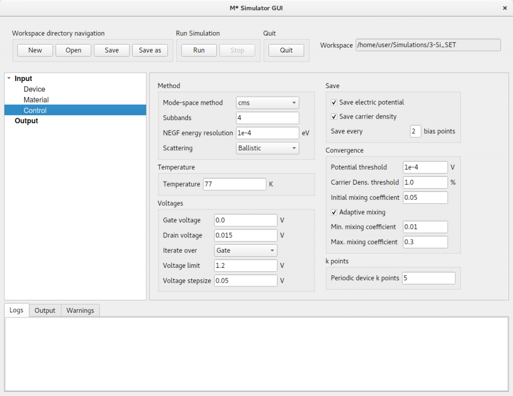
Control select coupled-mode space (CMS) as the mode-space method, as required for all devices with heterogeneous cross-sectional dimensions, and 4 subbands per valley. Since this device will exhibit strong state quantisation, we need to increase the resolution of the NEGF solver in order to capture states that are very narrow in energy; increase NEGF energy resolution to 10-4 eV to ensure an adequate description of the density of states throughout the device. Furthermore, set a temperature of 77 K and a drain voltage of 0.015 V for enhanced observation of quantum effects. A gate voltage sweep of [0.0,1.2] V in steps of 0.05 V is adequate to explore all regions of operation. Enable saving electric potentials and carrier densities, and set Save every [2] bias points to reduce disk space usage as saving data for every other bias point should provide enough data to study the device. Finally, set the same convergence parameters as in previous tutorials and shown in figure 3
Figure 4:In the Control panel, enter parameter values shown in the figure and discussed in the text.
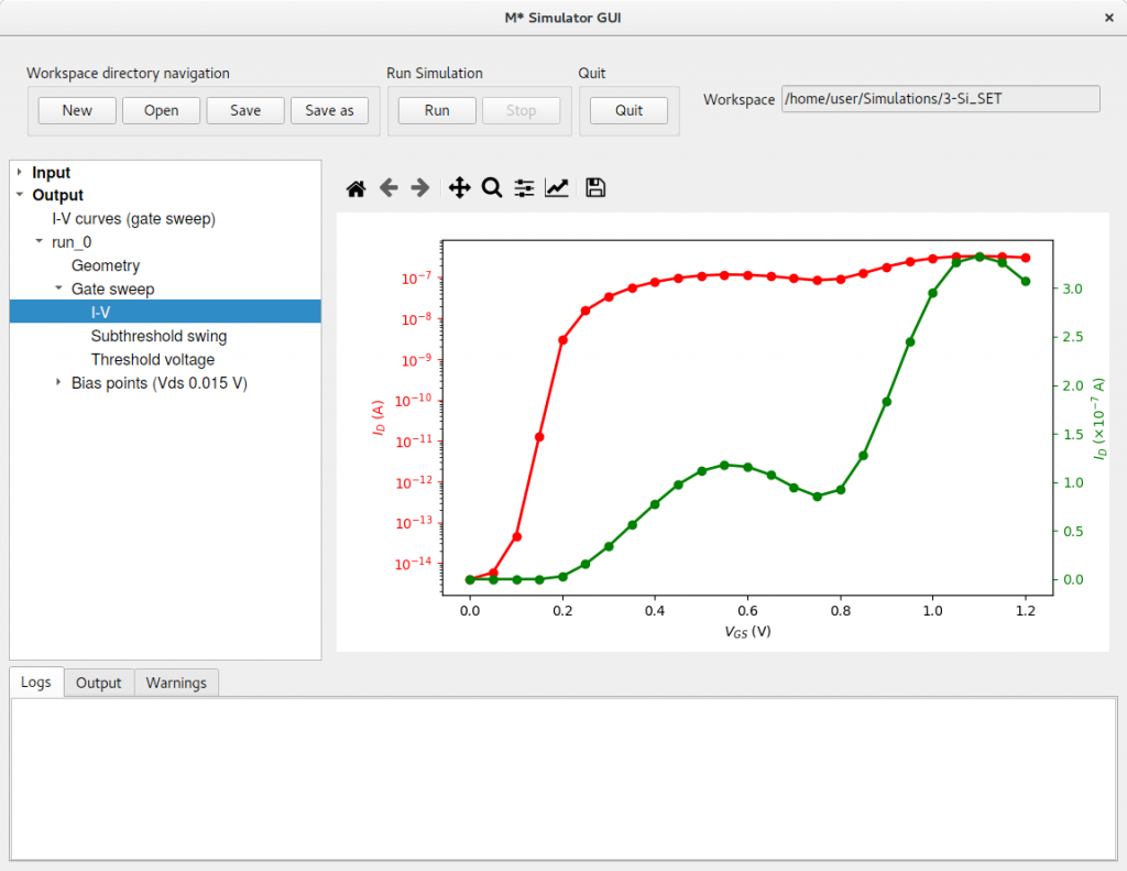
When you have finished setting up all input parameters, click Run to begin the simulation. You may follow the simulation’s progress tracking the content of the Logs tab in the bottom pane. You can inspect your simulation’s output as it progresses and bias points are converged; once it’s completed, you may plot the device’s ID – VGS characteristics as shown in figure 4: note the the oscillatory behaviour observed in the linear scale plot (green curve) for VGS > 0.2 V.
Figure 5:Si single-electron transistor’s transfer characteristics at T = 77 K.
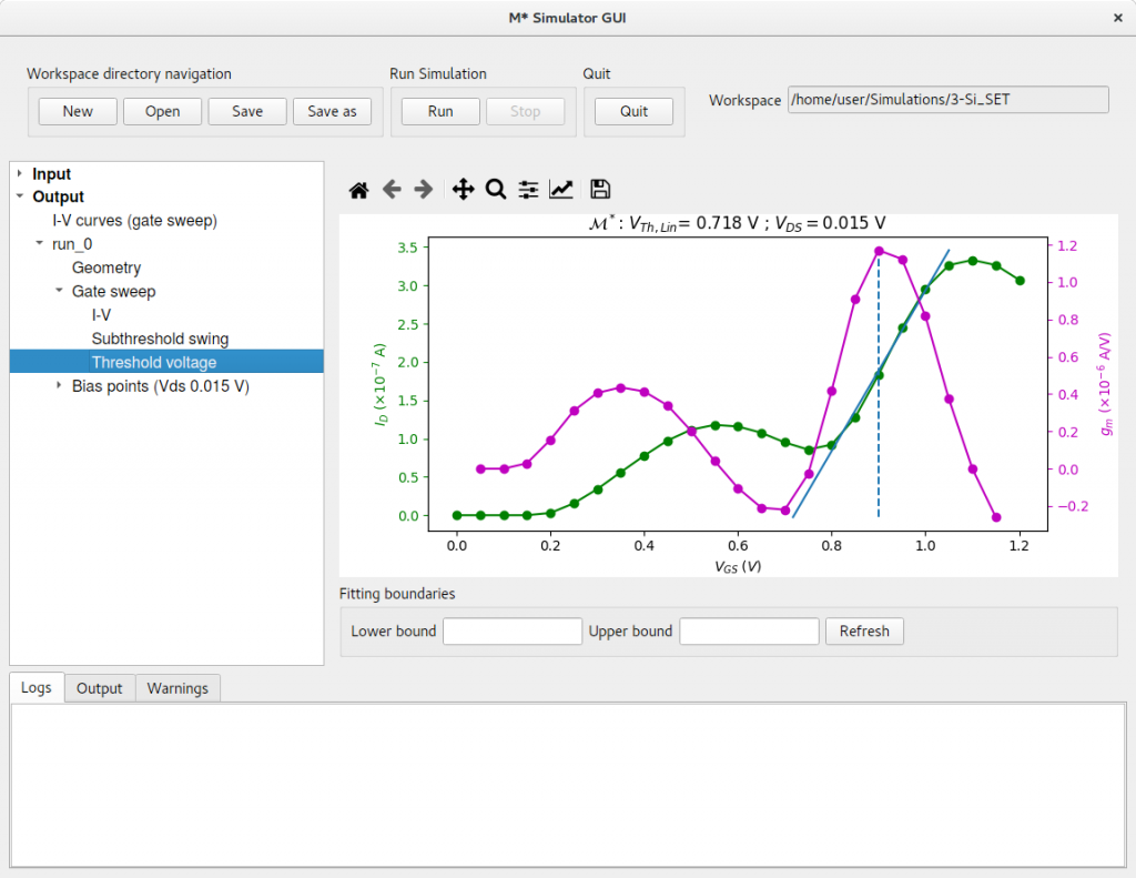
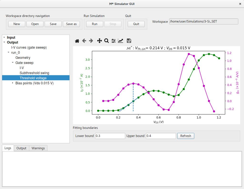
To begin investigating the properties of this device, let us calculate its threshold voltage by opening the corresponding panel Output->Threshold Voltage. You will observe the default algorithm does not correctly compute the threshold voltage as it interprets the device is turning ON around the [0.8,1.0] V range, as shown in figure 5. To obtain the correct threshold voltage, we need to manually set the Fitting boundaries at the bottom of the plot to indicate the linear regime corresponding to the first drain current increase observed in the plot (green curve). Enter values of 0.3 V and 0.4 V for the Lower bound and Upper bound fields, respectively, and click Refresh to obtain a plot similar to figure 6.
Figure 6:The default VTh extraction algorithm does not detect the correct settings for computing the SET’s threshold voltage.Figure 7:Setting manual fitting range allows computing the correct threshold voltage for this device.
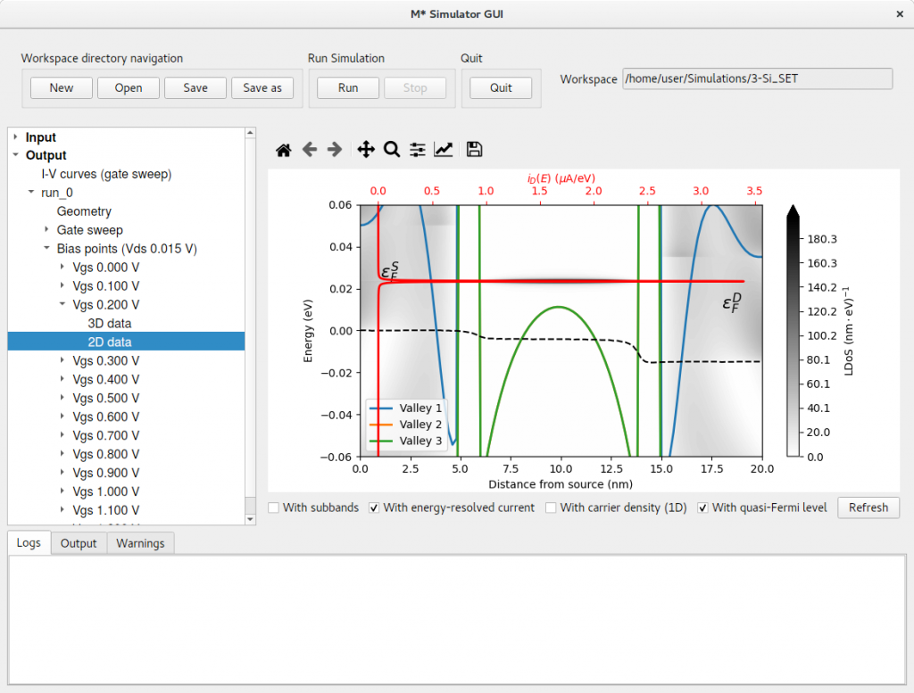
We shall now employ 2D data panels corresponding to a few values of the gate bias to understand the nature of drain current oscillations. Figure 7 shows the local density of states (LDoS), lowest-energy subband for each valley, energy-resolved current, and quasi-Fermi level along the device; as the gate-source bias increases and the first (i.e. lowest-energy) quantised state in the channel begins aligning with occupied states in the source, the device begins to turn ON.
Figure 8:LDoS, energy-resolved current, and quasi-Fermi level for VGS = 0.2 V.
Increasing the gate potential continues to shift states in the channel towards lower energies and the we encounter the first maximum in the ID – VGS characteristics when the lowest-energy quantised state in the channel enters the source-drain bias window (figure 08).
Figure 9:LDoS, energy-resolved current, and quasi-Fermi level for VGS = 0.5 V.
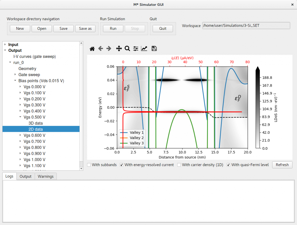
For larger gate-source biases, conduction through the second quantised state in the channel begins as it aligns with states occupied in the source, while conduction through the first state in the channel is suppressed due to its alignment with increasingly occupied states in the drain, as depicted in figure 9; this results in an overall reduction in the drain current observed in the VGS = [0.6,0.75] V range.
Figure 10:LDoS, energy-resolved current, and quasi-Fermi level for VGS = 0.8 V.
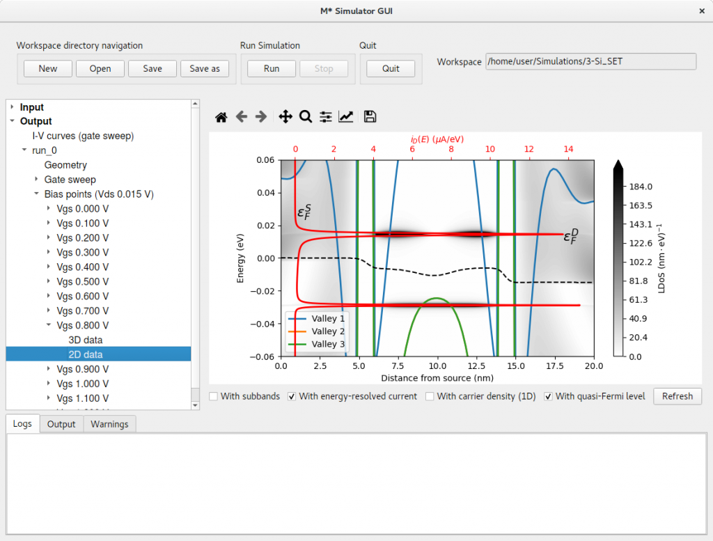
Further increases in the gate potential continue to suppress transport through the channel’s first quantised state until it becomes irrelevant for electron transport and the second quantised state in the channel dominates instead, as shown in figure 10.
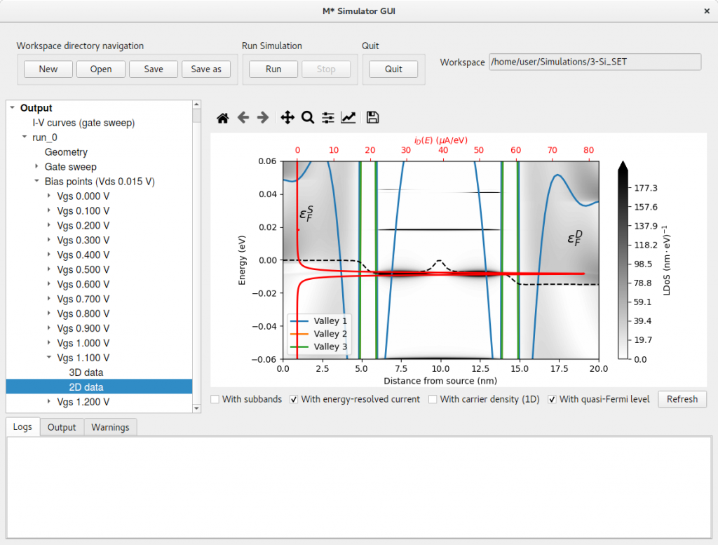
Figure 11:LDoS, energy-resolved current, and quasi-Fermi level for VGS = 1.1 V.
")